ZHCSIL2C July 2018 – March 2022 UCC24624
PRODUCTION DATA
- 1 特性
- 2 应用
- 3 说明
- 4 Revision History
- 5 说明(续)
- 6 Pin Configuration and Functions
- 7 Specifications
- 8 Detailed Description
- 9 Application and Implementation
- 10Power Supply Recommendations
- 11Layout
- 12Device and Documentation Support
8.3.1 Power Management
The UCC24624 synchronous-rectifier (SR) controller is powered from the REG pin through an internal linear regulator between the VDD pin and the REG pin. This configuration allows for optimal design of the gate driver stage to achieve fast driving speed, low driving loss and high noise immunity.
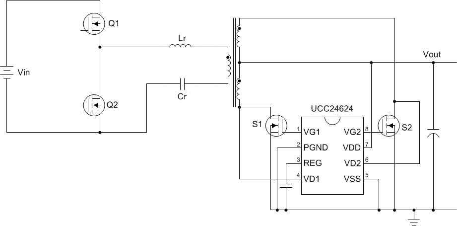
A typical application diagram of UCC24624 is shown in Figure 8-1. In most cases, the UCC24624 can be directly powered from the LLC resonant converter output (See Section 8.4.3 for more details). Both SR MOSFETs are located in the secondary side current return paths for easier voltage sensing, IC biasing, and gate driving.
 Figure 8-1 UCC24624 Application Diagram in LLC Resonant Converter
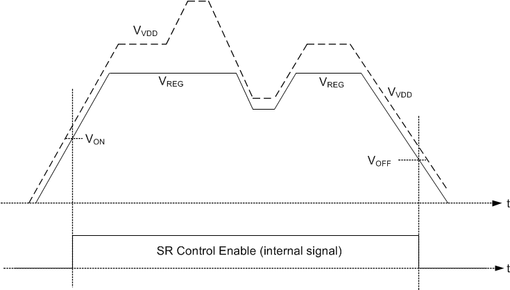
During start-up, the output voltage rises from 0 V. With the rise of the output voltage, the internal linear regulator operates in a pass-through mode, and the REG pin voltage rises together with the output voltage. The UVLO function of UCC24624 monitors the voltage on REG pin instead of VDD pin. Before the REG pin voltage increases above the UVLO on threshold (VREGON), UCC24624 consumes the minimum current of IVDDSTART. Once the REG pin voltage rises above the UVLO on threshold, the device starts to consume the full operating current, including IVDDRUN and the gate driving currents, and controls the on and off of the SR MOSFETs.
When VDD voltage is above approximately 11 V, the internal linear regulator operates in the regulator mode. The REG pin voltage is now well regulated to 11 V. This allows the optimal driving voltage for the SR MOSFET without increasing the gate driver loss for typical power MOSFETs. The internal regulator is rated at 30 mA of load regulation capability for higher switching frequency operation, or driving high SR MOSFET gate capacitances. It is required to have sufficient bypass capacitance on the REG pin to ensure stable operation of the linear regulator. A 2.2-μF X5R or better ceramic bypass capacitor is recommended.
When VDD voltage falls below 11 V, the internal linear regulator operates in the pass-through mode again. Depending on the load current, the regulator has a voltage drop of approximately 0.2 V. The UCC24624 continues to operate during this mode until the REG pin voltage drops below the UVLO turn-off level (VREGOFF).
A basic timing diagram of the VDD and the REG pin voltages can be found in Figure 8-2.
 Figure 8-2 Timing diagram for VDD and REG
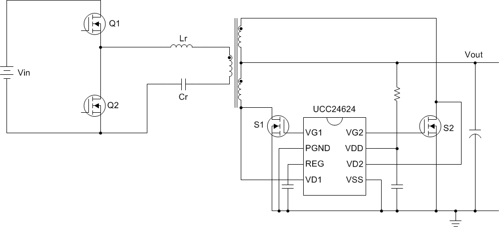
The UCC24624 VDD may be connected directly to the converter output when the output voltage is less than VDDCLAMP minimum value of 24.75 V. However, for the applications where the output voltage is higher than that level, including special conditions such as over voltage transients, the UCC24624 can still work with some simple modification. To allow UCC24624 to operate with higher output voltages, UCC24624 is equipped with an internal voltage clamp, at 27.5 V typical clamping voltage. Add a series resistor between the LLC converter output voltage and the UCC24624 VDD pin, as shown in Figure 8-3. This way the voltage on VDD is limited by the internal clamp. The clamp current must be kept less than 15 mA. For example, at 36-V output, use a resistor larger than 750 Ω. Because the gate drive voltage is only 11 V, this added resistor still allows enough voltage on the gate drive to maintain the reliable operation of the SRs. Furthermore, the current consumption of the SR controller is mainly caused by the SR MOSFET gate charge. The added resistor won't increase the power consumption if the clamping circuit is not activated. Instead, it relocates some loss from the UCC24624 to the resistor and improves the thermal handling of the UCC24624.
 Figure 8-3 UCC24624 Configuration for an Output Voltage Higher Than 24.75 V