ZHCSK64B October 2019 – December 2020 TPSM265R1
PRODUCTION DATA
- 1 特性
- 2 应用
- 3 说明
- 4 Revision History
- 5 Pin Configuration and Functions
-
6 Specifications
- 6.1 Absolute Maximum Ratings
- 6.2 ESD Ratings
- 6.3 Recommended Operating Conditions
- 6.4 Thermal Information
- 6.5 Electrical Characteristics
- 6.6 Typical Characteristics (VIN = 5 V)
- 6.7 Typical Characteristics (VIN = 12 V)
- 6.8 Typical Characteristics (VIN = 24 V)
- 6.9 Typical Characteristics (VIN = 48 V)
- 6.10 Typical Characteristics (VIN = 65 V)
-
7 Detailed Description
- 7.1 Overview
- 7.2 Functional Block Diagram
- 7.3
Feature Description
- 7.3.1 Adjustable Output Voltage (FB)
- 7.3.2 Input Capacitor Selection
- 7.3.3 Output Capacitor Selection
- 7.3.4 Precision Enable (EN), Undervoltage Lockout (UVLO), and Hysteresis (HYS)
- 7.3.5 PFM Operation
- 7.3.6 Power Good (PGOOD)
- 7.3.7 Configurable Soft Start (SS)
- 7.3.8 Overcurrent Protection (OCP)
- 7.3.9 Thermal Shutdown
- 7.4 Device Functional Modes
- 8 Applications and Implementation
- 9 Power Supply Recommendations
- 10Layout
- 11Device and Documentation Support
- 12Mechanical, Packaging, and Orderable Information
5 Pin Configuration and Functions
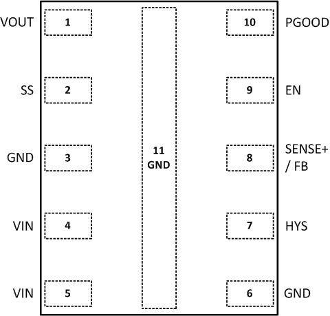
 Figure 5-1 10-Pin uSiP Exposed Thermal PadSIL-10C
Package(Top View)
Figure 5-1 10-Pin uSiP Exposed Thermal PadSIL-10C
Package(Top View)Table 5-1 Pin Functions
| PIN | TYPE(1) | DESCRIPTION | |
|---|---|---|---|
| NO. | NAME | ||
| 1 | VOUT | O | Output voltage pin. The VOUT pin is connected to the internal output inductor. Connect the VOUT pin to an external output capacitor and the output load. The output capacitor connections must be made as close as possible to the VOUT and GND pin 11 of the module. See Section 10.2. |
| 2 | SS | I | Soft-start programming pin. If the SS pin is floating, the output voltage ramp up time is approximately 1 ms after the device is enabled by the EN pin. If a 100-kΩ resistor is placed from the SS pin to GND, the internal soft start is disabled and the output voltage ramps up immediately after the device is enabled with the EN pin. Other output voltage ramp up times can be obtained by connecting an appropriate capacitance from the SS pin to GND. |
| 3, 6, 11 | GND | G | Ground pins. Connect all GND pins to the system ground plane. Pin 3 is not connected to GND internal to the module. Connect pin 3 directly to pin 11 on the host PCB. See Section 10.2. |
| 4, 5 | VIN | I | Input supply pins. The VIN pins are connected to the internal controller and power MOSFETs. Connect the VIN pins to an external input capacitor and the input power source. The input capacitor connections must be made as close as possible to the VIN pins and GND pin 6 of the module. See Section 10.2. |
| 7 | HYS | O | Enable hysteresis pin. The open-drain HYS pin can be used along with external resistors to program the hysteresis of a user-defined UVLO using the EN pin. HYS is internally pulled to GND when EN is below its turnon threshold and HYS goes open drain when EN is above its turnon threshold. |
| 8 | SENSE+/FB | I | Output voltage feedback pin. For fixed output voltage options, the SENSE+ pin must be externally connected to VOUT. For the adjustable output voltage option, the FB pin must be connected to an external resistor divider that is connected between VOUT and GND. |
| 9 | EN | I | Enable pin. The module is enabled when the EN pin is pulled high and disabled when the EN pin is pulled low. An external resistor divider can be connected to the EN pin to act as an external UVLO. |
| 10 | PGOOD | O | Power Good pin. The open-drain PGOOD pin is pulled low when the SENSE+ or FB pin is below the VOUT regulation target. An external 10-kΩ to 100-kΩ pullup resistor can be used to pull the PGOOD pin high when VOUT meets the regulation target. |
(1) G = Ground, I = Input, O = Output