ZHCSKB9Q December 1999 – October 2019 UCC1895 , UCC2895 , UCC3895
PRODUCTION DATA.
- 1 特性
- 2 应用
- 3 说明
- 4 修订历史记录
- 5 Pin Configuration and Functions
- 6 Specifications
-
7 Detailed Description
- 7.1 Overview
- 7.2 Functional Block Diagrams
- 7.3
Feature Description
- 7.3.1 ADS (Adaptive Delay Set)
- 7.3.2 CS (Current Sense)
- 7.3.3 CT (Oscillator Timing Capacitor)
- 7.3.4 DELAB and DELCD (Delay Programming Between Complementary Outputs)
- 7.3.5 EAOUT, EAP, and EAN (Error Amplifier)
- 7.3.6 OUTA, OUTB, OUTC, and OUTD (Output MOSFET Drivers)
- 7.3.7 PGND (Power Ground)
- 7.3.8 RAMP (Inverting Input of the PWM Comparator)
- 7.3.9 REF (Voltage Reference)
- 7.3.10 RT (Oscillator Timing Resistor)
- 7.3.11 GND (Analog Ground)
- 7.3.12 SS/DISB (Soft Start/Disable)
- 7.3.13 SYNC (Oscillator Synchronization)
- 7.3.14 VDD (Chip Supply)
- 7.4 Device Functional Modes
- 7.5 Programming
-
8 Application and Implementation
- 8.1 Application Information
- 8.2
Typical Application
- 8.2.1 Design Requirements
- 8.2.2
Detailed Design Procedure
- 8.2.2.1 Power Loss Budget
- 8.2.2.2 Preliminary Transformer Calculations (T1)
- 8.2.2.3 QA, QB, QC, QD FET Selection
- 8.2.2.4 Selecting LS
- 8.2.2.5 Selecting Diodes DB and DC
- 8.2.2.6 Output Inductor Selection (LOUT)
- 8.2.2.7 Output Capacitance (COUT)
- 8.2.2.8 Select Rectifier Diodes
- 8.2.2.9 Input Capacitance (CIN)
- 8.2.2.10 Current Sense Network (CT, RCS, RR, DA)
- 8.2.3 Application Curves
- 9 Power Supply Recommendations
- 10Layout
- 11器件和文档支持
- 12机械、封装和可订购信息
8.2.2.10.5 Setting the Switching Delays
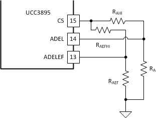
Higher power designs will benefit from the adaptive delays provided by the ADS pin but that feature is not used in this example. Setting RADSH = 0 Ω defeats the adaptive delay and a fixed value for tDELAB and tDELCD is used. If it is planned to use the adaptive delay feature then the resistor RADSL should be included in the layout but not populated until delay optimisation is being done on actual hardware.
 Figure 20. UCC3895 Adaptive Delays
 We set the delay times as follows. The resonant frequency of the shim inductor LS with the stray capacitance at the switched node is given by:

Set the initial tABSET and tCDSET values to half the resonant period

The resistors RAB and RCD are given by a modified version of Equation 5 and Equation 6.

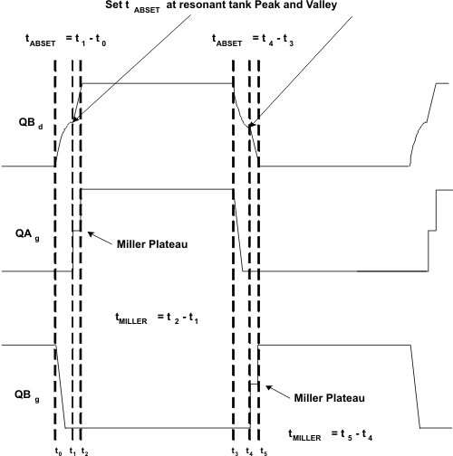
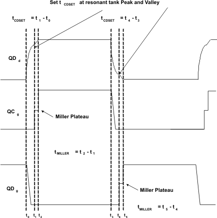
It is important to recognise that the delay times set by RAB and RCD are those measured at the device pins. Propagation delays mean that the delay times seen at the primary of the transformer will be different and this is the reason why the delays have to be optimised on actual hardware. Once the prototype is up and running it is recommended that you fine tune tABSET and tCDSET at light load. Refer to Figure 21 and Figure 22. It is easier to achieve ZVS at the drain of QD than at the drain of QA because the output inductor current reflected in the transformer primary is greater at QD and QC turn-off than it is at QA and QB turn-off.
 Figure 21. tABSET to Achieve Valley Switching at Light Loads
  Figure 22. tCDSET to Achieve Valley Switching at Light Loads