ZHCSMV7B February 2020 – May 2021 ISO1640 , ISO1641
PRODUCTION DATA
- 1 特性
- 2 应用
- 3 说明
- 4 Revision History
- 5 Pin Configuration and Functions
-
6 Specifications
- 6.1 Absolute Maximum Ratings
- 6.2 ESD Ratings
- 6.3 Recommended Operating Conditions
- 6.4 Thermal Information
- 6.5 Power Ratings
- 6.6 Insulation Specifications
- 6.7 Safety-Related Certifications
- 6.8 Safety Limiting Values
- 6.9 Electrical Characteristics
- 6.10 Supply Current Characteristics
- 6.11 Timing Requirements
- 6.12 I2C Switching Characteristics
- 6.13 GPIO Switching Characteristics
- 6.14 Insulation Characteristics Curves
- 6.15 Typical Characteristics
- 7 Parameter Measurement Information
- 8 Detailed Description
- 9 Application and Implementation
- 10Power Supply Recommendations
- 11Layout
- 12Device and Documentation Support
- 13Mechanical, Packaging, and Orderable Information
9.2.2 Detailed Design Procedure
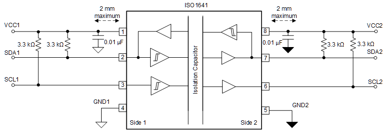
Although the ISO1640 features bidirectional data channels, the device performs optimally when side 1 (SDA1 and SCL1) is connected to a single controller or node of an I2C network while side 2 (SDA2 and SCL2) is connected to the I2C bus.
The power-supply capacitor with a value of 0.1-µF must be placed as close to the power supply pins as possible. The recommended placement of the capacitors must be 2-mm maximum from input and output power supply pins (VCC1 and VCC2).
The maximum load permissible on the input lines, SDA1 and SCL1, is ≤ 80 pF and on the output lines, SDA2 and SCL2, is ≤ 400 pF.
The minimum pullup resistors on the input lines, SDA1 and SCL1 to VCC1 must be selected in such a way that input current drawn is ≤ 3.5 mA. The minimum pullup resistors on the input lines, SDA2 and SCL2, to VCC2 must be selected in such a way that output current drawn is ≤ 50 mA. The maximum pullup resistors on the bus lines (SDA1 and SCL1) to VCC1 and on bus lines (SDA2 and SCL2) to VCC2, depends on the load and rise time requirements on the respective lines to comply with I2C protocols. For more information, see https://www.ti.com/lit/an/slva689/slva689.pdf.
The output waveforms for SDA1 and SCL1 are captured on the oscilloscope focusing on the low VOL1 voltage offset offered with the ISO164x. This voltage offset is due to the high output low level on side 1 designed to prevent a latch-up state mentioned in Section 8.4.
 Figure 9-5 Typical ISO1640 Circuit Hookup
 Figure 9-6 Typical ISO1641 Circuit Hookup