TPS7A470x 36V,1A,4µVRMS,射频 (RF) 低压降 (LDO) 电压稳压器
1 特性
- 输入电压范围:+3V 至 +36V
- 输出电压噪声:
4µVRMS(10Hz,100Hz) - 电源纹波抑制:
- 82dB (100Hz)
- ≥ 55dB (10Hz,10MHz)
- 两个输出电压模式:
- ANY-OUT™ 版本(借助印刷电路板 (PCB) 布局布线的用户可调输出):
- 无需外部反馈电阻器或者前馈电容器
- 输出电压范围:+1.4V 至 +20.5V
- 可调版本(仅适用于 TPS7A4701):
- 输出电压范围:+1.4V 至 +34V
- ANY-OUT™ 版本(借助印刷电路板 (PCB) 布局布线的用户可调输出):
- 输出电流:1A
- 压降电压:1A 时为 307mV
- 与 CMOS 逻辑电平兼容的启用引脚
- 内置固定电流限制和
热关断 - 采用高性能散热封装:5mm × 5mm 四方扁平无引线 (QFN)
- 工作温度范围:
–40°C 至 125°C
2 应用
- 压控振荡器 (VCO)
- 频率合成器
- 测试和测量
- 仪器仪表、医疗和音频
- RX,TX,和 PA 电路
- 用于运算放大器,
数模转换器 (DAC),模数转换器 (ADC),和其它高精度模拟电路的电源轨 - 后置 DC/DC 转换器稳压和
纹波滤除 - 基站和电信基础设施
- +12V 和 +24V 工业用总线
3 说明
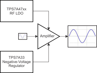
TPS7A47 是一款正电压 (+36V) 超低噪声 (4µVRMS) 低压降线性稳压器 (LDO) 系列米6体育平台手机版_好二三四,能够提供 1A 负载。
用户可通过印刷电路板 (PCB) 布局布线来编程设定 TPS7A4700 输出电压(最高 20.5V),无需外部电阻器或前馈电容器,从而减少了元件总数量。
配置 TPS7A4701 输出电压时,用户可通过 PCB 布局编程设定(高达 20.5V)或使用外部反馈电阻器调节(高达 34V)。
TPS7A47 由双极型技术设计而成,主要用于高准确度、高精度仪器仪表应用。在此类应用中,规整的电压轨对于系统性能的最大化至关重要。 这种设计使其成为功率运算放大器,模数转换器(ADC),数模转换器 (DAC) 及其它关键应用(诸如医疗、射频 (RF) 和测试测量应用)中高性能模拟电路的最佳选择。
此外,TPS7A47 线性稳压器也非常适合于后置 DC/DC 转换器稳压。 通过滤除 dc/dc 开关转换所固有的输出电压纹波,可确保在灵敏仪器仪表、测试和测量、音频和 RF 应用中将系统性能最大化。
对于需要正向和负向低噪声电源轨的应用,请考虑 TI 的TPS7A33负向高电压、超低噪声线性稳压器系列米6体育平台手机版_好二三四。
器件信息(1)
| 部件号 | 封装 | 封装尺寸(标称值) |
|---|---|---|
| TPS7A470x | VQFN (20) | 5mm x 5mm |
- 如需了解所有可用封装,请见数据表末尾的可订购米6体育平台手机版_好二三四附录。
4 修订历史记录
Changes from E Revision (January 2014) to F Revision
- Added 处理额定值表、特性描述部分、器件功能模式、应用和实施部分、电源相关建议部分、布局部分、器件和文档支持部分以及机械、封装和可订购信息部分Go
- 重新编写了特性列表中的第九个要点Go
- Changed polarity of op amp shown on right side of the functional block diagram Go
- Reworded second paragraph in Soft-Start And Inrush Current section Go
- Revised Capacitor Recommendations sectionGo
- Changed paragraph 2 of Dropout Voltage (VDO) section for clarity Go
- Revised paragraph 1 of Startup section Go
- Rewrote paragraph 1 of Power-Supply Rejection Ratio (PSRR) section to eliminate confusion Go
- Changed paragraph 1 of Power Supply Recommendations section Go
- Changed paragraph 1 and paragraph 4 of Power Dissipation (PD) sectionGo
- Revised paragraph 2 of Layout Guidelines section Go
- Changed second paragraph of Thermal Protection section Go
Changes from D Revision (December 2013) to E Revision
- 标题页的三个实例中输出电压噪声值从 4.17µV 改为 4µVGo
- 更改了说明部分中的第二段和第三段Go
- Added "Thermal Pad" to pin configuration drawingGo
- Changed EN pin descriptionGo
- Changed SENSE/FB pin to be for TPS7A4701 onlyGo
- Added new row to Pin Descriptions table for SENSE pin (for TPS7A4700 only)Go
- Added new row to Pin Descriptions table for thermal padGo
- Added VREF parameterGo
- Added TPS7A4701 device to test conditions for VNR parameterGo
- Added Feedback Pin Current parameter to Electrical Characteristics Go
- Deleted Dropout Voltage vs Output Current graphGo
- Added EN pin to Functional Block DiagramGo
- Added sentence to ANY-OUT Programmable Output Voltage section to clarify ANY-OUT is for both devicesGo
- Changed last two paragraphs of Adjustable Operation sectionGo
- Added "TPS7A4701 Only" to Adjustable Operation section titleGo
- Deleted equation in Figure 23Go
- Changed Equation 3Go
Changes from C Revision (July 2013) to D Revision
- 将数据表状态从生产结构更改为生产数据Go
- 已将 TPS7A4701 静电放电 (ESD) 额定值从 > 1kV 更改为 2.5kVGo
- Changed noise reduction pin voltage parameter to show both devicesGo
- Added text clarifying VREF typical value to last paragraph on pageGo
Changes from B Revision (April 2013) to C Revision
- 从数据表中删除了 TPS7A4702 预览器件Go
Changes from A Revision (July 2012) to B Revision
- 已将 TPS7A47 改为 TPS7A4700Go
- 已将 TPS7A4701 和 TPS7A4702 预览器件添加到数据表中Go
- 更改了标题页图表Go
- Added FB to SENSE pin to Functional Block DiagramGo
- Added new paragraph after Table 1Go
- Added new Table 2Go
- Added Adjustable Operation sectionGo
Changes from * Revision (June 2012) to A Revision
- 已移动到全生产数据(在整个文档中进行更改)Go
5 Pin Configuration and Functions
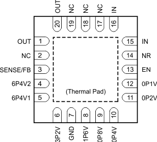
Pin Functions
| PIN | I/O | DESCRIPTION | |
|---|---|---|---|
| NAME | NO. | ||
| 0P1V | 12 | I | When connected to GND, this pin adds 0.1 V to the nominal output voltage of the regulator. |
| Do not connect any voltage other than GND to this pin. If not used, leave this pin floating. | |||
| 0P2V | 11 | I | When connected to GND, this pin adds 0.2 V to the nominal output voltage of the regulator. |
| Do not connect any voltage other than GND to this pin. If not used, leave this pin floating. | |||
| 0P4V | 10 | I | When connected to GND, this pin adds 0.4 V to the nominal output voltage of the regulator. |
| Do not connect any voltage other than GND to this pin. If not used, leave this pin floating. | |||
| 0P8V | 9 | I | When connected to GND, this pin adds 0.8 V to the nominal output voltage of the regulator. |
| Do not connect any voltage other than GND to this pin. If not used, leave this pin floating. | |||
| 1P6V | 8 | I | When connected to GND, this pin adds 1.6 V to the nominal output voltage of the regulator. |
| Do not connect any voltage other than GND to this pin. If not used, leave this pin floating. | |||
| 3P2V | 6 | I | When connected to GND, this pin adds 3.2 V to the nominal output voltage of the regulator. |
| Do not connect any voltage other than GND to this pin. If not used, leave this pin floating. | |||
| 6P4V1 | 5 | I | When connected to GND, this pin adds 6.4 V to the nominal output voltage of the regulator. |
| Do not connect any voltage other than GND to this pin. If not used, leave this pin floating. | |||
| 6P4V2 | 4 | I | When connected to GND, this pin adds 6.4 V to the nominal output voltage of the regulator. |
| Do not connect any voltage other than GND to this pin. If not used, leave this pin floating. | |||
| EN | 13 | I | Enable pin. The device is enabled when the voltage on this pin exceeds the maximum enable voltage, VEN(HI). If enable is not required, tie EN to IN. |
| GND | 7 | — | Ground |
| IN | 15, 16 | I | Input supply. A capacitor greater than or equal to 1 µF must be tied from this pin to ground to assure stability. A 10-µF capacitor is recommended to be connected from IN to GND (as close to the device as possible) to reduce circuit sensitivity to printed circuit board (PCB) layout, especially when long input traces or high source impedances are encountered. |
| NC | 2, 17-19 | — | This pin can be left open or tied to any voltage between GND and IN. |
| NR | 14 | — | Noise reduction pin. When a capacitor is connected from this pin to GND, RMS noise can be reduced to very low levels. A capacitor greater than or equal to 10 nF must be tied from this pin to ground to assure stability. A 1-µF capacitor is recommended to be connected from NR to GND (as close to the device as possible) to maximize ac performance and minimize noise. |
| OUT | 1, 20 | O | Regulator output. A capacitor greater than or equal to 10 µF must be tied from this pin to ground to assure stability. A 47-µF ceramic output capacitor is highly recommended to be connected from OUT to GND (as close to the device as possible) to maximize ac performance. |
| SENSE/FB | 3 | I | Control-loop error amplifier input (TPS7A4701 only). |
| This is the SENSE pin if the device output voltage is programmed using ANY-OUT (no external feedback resistors). This pin must be connected to OUT. Connect this pin to the point of load to maximize accuracy. | |||
| This is the FB pin if the device output voltage is set using external resistors. See the Adjustable Operation section for more details. | |||
| SENSE | 3 | I | Control-loop error amplifier input (TPS7A4700 only). |
| This is the SENSE pin of the device and must be connected to OUT. Connect this pin to the point of load to maximize accuracy. | |||
| Thermal Pad | — | Connect the thermal pad to a large-area ground plane. The thermal pad is internally connected to GND. | |