SLVS363G August 2001 – September 2016 TPS3103 , TPS3106 , TPS3110
PRODUCTION DATA.
- 1 Features
- 2 Applications
- 3 Description
- 4 Revision History
- 5 Available Options
- 6 Pin Configuration and Functions
- 7 Specifications
- 8 Detailed Description
- 9 Application and Implementation
- 10Power Supply Recommendations
- 11Layout
- 12Device and Documentation Support
- 13Mechanical, Packaging, and Orderable Information
1 Features
-
Precision Supply Voltage Supervision Range:
0.9 V, 1.2 V, 1.5 V, 1.6 V, 2 V, and 3.3 V - High Trip-Point Accuracy: 0.75%
- Supply Current of 1.2 μA (Typical)
- RESET Defined With Input Voltages as Low as 0.4 V
- Power-On Reset Generator With a Delay Time of 130 ms
- Push/Pull or Open-Drain RESET Outputs
- Package Temperature Range: –40°C to 125°C
2 Applications
- Applications Using Low-Power DSPs, Microcontrollers, or Microprocessors
- Portable and Battery-Powered Equipment
- Intelligent Instruments
- Wireless Communication Systems
- Industrial Equipment
- Notebook and Desktop Computers
3 Description
The TPS310x and TPS311x families of supervisory circuits provide circuit initialization and timing supervision, primarily for DSP and processor-based systems.
During power-on, RESET is asserted low when the supply voltage (VDD) becomes higher than 0.4 V. Thereafter, the supervisory circuit monitors VDD and keeps the RESET output low as long as VDD remains below the threshold voltage (VIT–). To ensure proper system reset, after VDD surpasses the threshold voltage, an internal timer delays the transition of the RESET signal from low to high for the specified time. When VDD drops below VIT–, the output transitions low again.
All the devices of this family have a fixed-sense threshold voltage (VIT–) set by an internal voltage divider.
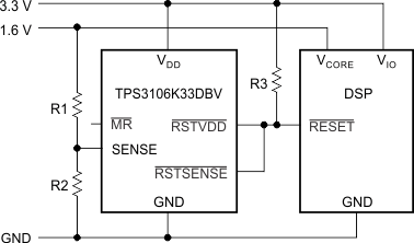
The TPS3103 and TPS3106 devices have an active-low, open-drain RESET output and either an integrated power-fail input (PFI) or SENSE input with corresponding outputs for monitoring other voltages. The TPS3110 has an active-low push/pull RESET and a watchdog timer to monitor the operation of microprocessors. All three devices have a manual reset pin that can be used to force the outputs low regardless of the sensed voltages.
The product spectrum is designed for supply voltages of 0.9 V up to 3.6 V. The circuits are available in 6-pin SOT-23 packages. The TPS31xx family is characterized for operation over a temperature range of –40°C to 125°C.
Device Information(1)
| PART NUMBER | PACKAGE | BODY SIZE (NOM) |
|---|---|---|
| TPS3103xxx | SOT-23 (6) | 2.90 mm × 1.60 mm |
| TPS3106xxx | ||
| TPS3110xxx |
- For all available packages, see the orderable addendum at the end of the data sheet.
4 Revision History
Changes from F Revision (November 2015) to G Revision
- Changed Package Temperature Range Features bullet to extend to 125°C Go
- Changed supply voltage and temperature range in last paragraph of Description section Go
- Changed maximum specifications in Supply voltage, All other pins, and Operating temperature parameters in Absolute Maximum Ratings tableGo
- Changed maximum specifications in VDD, PFI, and TJ parameters of Recommended Operating Conditions tableGo
- Added TA = –40°C to 125°C rows to VIT– parameter of Electrical Characteristics tableGo
- Added second row to VIT–(S) parameter of Electrical Characteristics tableGo
- Changed IDD parameter of Electrical Characteristics tableGo
- Changed Typical Characteristics curves TPS3110E09 Supply Current vs Supply Voltage, TPS3110E09 Low-Level Output Voltage vs Low-Level Output Current, TPS3110E09 Low-Level Output Voltage vs Low-Level Output Current, TPS3110E09 High-Level Output Voltage vs High-Level Output Current, and TPS3110K33 High-Level Output Voltage vs High-Level Output Current Go
- Changed Normalized Threshold Voltage vs Free-Air Temperature curveGo
- Changed supply voltage range in first sentence of Overview section Go
- Changed supply voltage range in description of Application Information section Go
- Changed Normalized Threshold Voltage vs Free-Air Temperature figureGo
- Changed supply voltage range in first sentence of Power Supply Recommendations sectionGo
Changes from E Revision (September 2007) to F Revision
- Added ESD Ratings table, Feature Description section, Device Functional Modes, Application and Implementation section, Power Supply Recommendations section, Layout section, Device and Documentation Support section, and Mechanical, Packaging, and Orderable Information section Go
- Changed title of document Go
- Deleted Features bullet for SOT23-6 package Go
- Changed front-page figureGo
- Changed second paragraph of Description section Go
- Changed fourth paragraph of Description sectionGo
- Changed Pin Configuration and Functions section; updated table format Go
- Changed "free-air temperature" to "junction temperature" in Absolute Maximum Ratings condition statementGo
- Deleted clamp current from Absolute Maximum Ratings table; changed to currentGo
- Deleted soldering temperature specification from Absolute Maximum Ratings tableGo
- Changed "free-air temperature" to "junction temperature" in Recommended Operating Conditions condition statement Go
- Added Thermal Information table; deleted Dissipation Ratings tableGo
- Changed "free-air temperature" to "junction temperature" in Electrical Characteristics condition statement Go
- Changed Switching Characteristics tableGo
- Changed Figure 1 title and timing drawing Go
- Changed Figure 2 titleGo
- Changed Figure 3Go
- Changed Figure 4Go
