ZHCSBG4B May 2013 – February 2019 ADS8862
PRODUCTION DATA.
- 1 特性
- 2 应用
- 3 说明
- 4 修订历史记录
- 5 Device Comparison Table
- 6 Pin Configuration and Functions
- 7 Specifications
- 8 Parameter Measurement Information
- 9 Detailed Description
- 10Application and Implementation
- 11Power Supply Recommendations
- 12Layout
- 13器件和文档支持
- 14机械、封装和可订购信息
封装选项
机械数据 (封装 | 引脚)
散热焊盘机械数据 (封装 | 引脚)
- DRC|10
订购信息
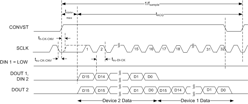
7.8 Timing Requirements: Daisy-Chain
all specifications are at AVDD = 3 V, DVDD = 3 V, and over the operating free-air temperature range (unless otherwise noted)| MIN | TYP | MAX | UNIT | |||
|---|---|---|---|---|---|---|
| tACQ | Acquisition time | 540 | ns | |||
| tconv | Conversion time | 500 | 930 | ns | ||
| 1/fsample | Time between conversions | 1470 | ns | |||
| tsu-CK-CNV | Setup time: SCLK valid to CONVST rising edge | 5 | ns | |||
| th-CK-CNV | Hold time: SCLK valid from CONVST rising edge | 5 | ns | |||
| tsu-DI-CNV | Setup time: DIN low to CONVST rising edge (see Figure 2) | 7.5 | ns | |||
| th-DI-CNV | Hold time: DIN low from CONVST rising edge (see Figure 61) | 0 | ns | |||
| tsu-DI-CK | Setup time: DIN valid to SCLK falling edge | 1.5 | ns | |||
 Figure 1. 3-Wire Operation: CONVST Functions as Chip Select
 NOTE: Figure 1 shows the timing diagram for the 3-Wire CS Mode Without a Busy Indicator interface option. However, the timing parameters specified in Timing Requirements: 3-Wire Operation table are also applicable for the 3-Wire CS Mode With a Busy Indicator interface option, unless otherwise specified; see the Device Functional Modes section for specific details for each interface option.
 Figure 2. 4-Wire Operation: DIN Functions as Chip Select
 NOTE: Figure 2 shows the timing diagram for the 4-Wire CS Mode Without a Busy Indicator interface option. However, the timing parameters specified in Timing Requirements: 4-Wire Operation table are also applicable for the 4-Wire CS Mode With a Busy Indicator interface option, unless otherwise specified; see the Device Functional Modes section for specific details for each interface option.
 Figure 3. Daisy-Chain Operation: Two Devices
 NOTE: Figure 3 shows the timing diagram for the Daisy-Chain Mode Without a Busy Indicator interface option. However, the timing parameters specified in Timing Requirements: Daisy-Chain table are also applicable for the Daisy-Chain Mode With a Busy Indicator interface option, unless otherwise specified; see the Device Functional Modes section for specific details for each interface option.