ZHCSGC8A March 2014 – June 2017 AFE5401-Q1
PRODUCTION DATA.
- 1 特性
- 2 应用
- 3 说明
- 4 修订历史记录
- 5 Pin Configuration and Functions
-
6 Specifications
- 6.1 Absolute Maximum Ratings
- 6.2 ESD Ratings
- 6.3 Recommended Operating Conditions
- 6.4 Thermal Information
- 6.5 Electrical Characteristics
- 6.6 Digital Characteristics
- 6.7 Timing Requirements: Output Interface
- 6.8 Timing Requirements: RESET
- 6.9 Timing Requirements: Serial Interface Operation
- 6.10 Typical Characteristics
- 7 Parameter Measurement Information
-
8 Detailed Description
- 8.1 Overview
- 8.2 Functional Block Diagram
- 8.3 Feature Description
- 8.4 Device Functional Modes
- 8.5 Programming
- 8.6 Register Maps
- 9 Application and Implementation
- 10Power Supply Recommendations
- 11Layout
- 12器件和文档支持
- 13机械、封装和可订购信息
8 Detailed Description
8.1 Overview
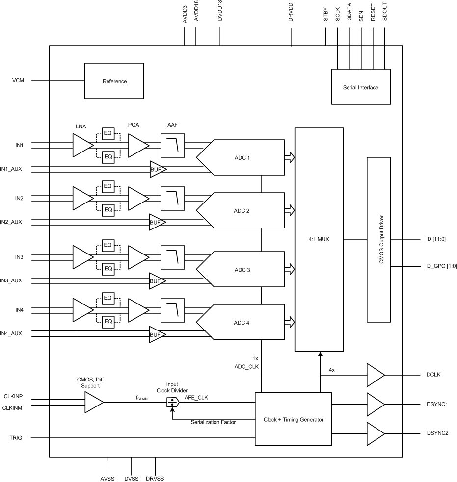
The AFE5401-Q1 is a very low-power, CMOS, monolithic, quad-channel, analog front-end (AFE). The signal path of each channel consists of a differential low-noise amplifier (LNA) followed by a differential programmable gain amplifier (PGA) in series with a differential antialias filter. The antialiasing filter output is sampled by a 12-bit, pipeline, analog-to-digital converter (ADC) based on a switched-capacitor architecture. Each ADC can also be differentially driven from INIP_AUX, INIM_AUX through an on-chip buffer (thus bypassing the LNA, PGA, and antialiasing filter).
Each block in the channel operates with a maximum 2-VPP output swing. Each PGA has a programmable gain range from 0 dB to 30 dB, with a resolution of 3 dB.
After the input signals are captured by the sampling circuit, the samples are sequentially converted by a series of low-resolution stages inside the pipeline ADC at the clock rising edge. The outputs of these stages are combined in a digital logic block to form the final 12-bit word with a latency of 10.5 tAFE_CLK clock cycles. The 12-bit words of all active channels are multiplexed and output as parallel CMOS levels. In addition to the data streams, a CMOS clock (DCLK) is also output. This clock must be used by the digital receiver [such as a digital signal processor (DSP)] to latch the AFE output parallel CMOS data.
8.2 Functional Block Diagram
8.3 Feature Description
8.3.1 Low-Noise Amplifier (LNA)
The analog input signal is buffered and amplified by an on-chip LNA. LNA gain is programmable with the LNA_GAIN register, as shown in Table 6.
Table 6. LNA_GAIN Register
| LNA_GAIN | DESCRIPTION (dB) | LNA_GAIN_Linear |
|---|---|---|
| 0 | 15 | 5.5 |
| 1 | 18 | 8 |
| 2 | 12 | 4 |
| 3 | 16.5 | 6.5 |
The LNA output is internally limited to 2 VPP. Thus, the maximum-supported input peak-to-peak swing is set by 2 V / LNA_GAIN_Linear.
Input-referred noise in default mode is 2.9 nV/√Hz at 30-dB PGA gain and 15-dB LNA gain. Input-referred noise can be further improved to 2.5 nV/√Hz by enabling the HIGH_POW_LNA register bit. However, this noise reduction results in increased power dissipation.
8.3.2 Programmable Gain Amplifier (PGA)
The PGA amplifies the analog input signal by a programmable gain. Gain can be programmed using the PGA_GAIN register, common to all channels, in 3-dB steps with a gain range of 30 dB. In default mode, PGA gain ranges from 0 dB to 30 dB. In equalizer mode, PGA gain ranges from 15 dB to 45 dB. PGA_GAIN register settings are listed in Table 7. Figure 57 shows the typical SNR values across PGA gain.
Table 7. PGA_GAIN Register Settings
| PGA_GAIN Settings | PGA GAIN IN DEFAULT MODE (dB) | PGA GAIN IN EQUALIZER MODE (dB) |
|---|---|---|
| 0 (0 dB) | 0.0 | 15.0 |
| 1 (3 dB) | 2.9 | 17.9 |
| 2 (6 dB) | 6.0 | 21.0 |
| 3 (9 dB) | 8.8 | 23.8 |
| 4 (12 dB) | 11.9 | 26.9 |
| 5 (15 dB) | 14.8 | 29.8 |
| 6 (18 dB) | 17.9 | 32.9 |
| 7 (21 dB) | 20.8 | 35.8 |
| 8 (24 dB) | 23.9 | 38.9 |
| 9 (27 dB) | 26.8 | 41.8 |
| 10 (30 dB) | 29.9 | 44.9 |
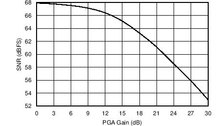 Figure 57. SNR Across PGA Gain
8.3.3 Antialiasing Filter
The device introduces a third-order, elliptic, active, antialias, low-pass filter (LPF) in the analog signal path. The filter –3-dB corner frequency can be configured using the FILTER_BW register, as shown in Table 8. The corresponding frequency response plots are shown in Figure 58 and Figure 59.
Table 8. FILTER_BW Register
| FILTER_BW | CORNER FREQUENCY (MHz) |
|---|---|
| 0 | 8 |
| 1 | 7 |
| 2 | 10.5 |
| 3 | 12 |
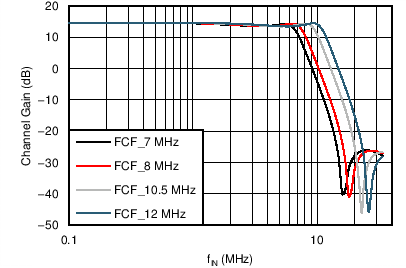
(PGA Gain = 0 dB)
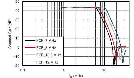
(PGA Gain = 30 dB)
8.3.4 Analog-to-Digital Converter (ADC)
The filtered analog input signal is sampled and converted into a digital equivalent code using a high-speed, low-power, 12-bit, pipeline ADC. The digital output of the device has a latency of 10.5 tAFE_CLK cycles because of the pipeline nature of the ADC. The digitized output of the device is in binary twos complement (BTC) format. The output format can be changed to offset binary format with the OFF_BIN_DATA_FMT register bit.
8.3.5 Digital Gain
The ADC output can be incremented digitally using a digital gain block. Digital gain is common for all channels and can be configured by enabling MULT_EN and applying the desired DIG_GAIN. Channel gain is given by Equation 1:
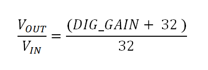
where
- (DIG_GAIN + 32) is the mod 128 number.
Figure 60 shows the typical digital gain curve for different DIG_GAIN values.
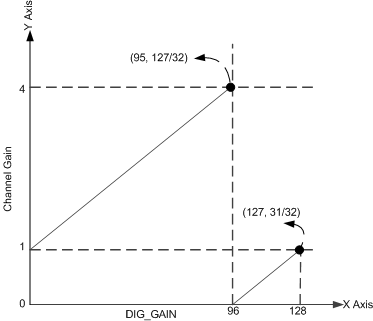 Figure 60. Digital Gain Graph
8.3.6 Input Clock Divider
The device clock input is passed through a clock divider block that can divide the input clock by a factor of 1, 2, 3, or 4. This divided clock (AFE_CLK) is used for simultaneously sampling the four ADC inputs. In default mode, a division factor of 1 is used where the AFE_CLK frequency is the same as the input clock frequency. The clock divider block can be enabled using the DIV_EN register bit and, when enabling this bit, the AFE_CLK frequency is automatically determined by the serialization factor set by the CH_OUT_DIS register bits (Table 12). The division factor can also be manually specified by enabling the DIV_FRC and DIV_REG register bits. Care must be taken to ensure that the input clock frequency is within the recommended operating range specified in the Recommended Operating Conditions.
After device reset, the divider is reset at the first pulse applied on the TRIG pin. This configuration is especially useful when using multiple devices in the system, where the sampling instants of all ADCs in the system must be synchronized. Figure 61 illustrates the TRIG timing diagram and the various divided-down AFE_CLK signals. Figure 62 provides the TRIG input setup and hold time with respect to the device clock input. Bit settings for the DIV_EN register, DIV_FRD register, and DIV_REG register are provided in Table 9, Table 10, and Table 11, respectively.
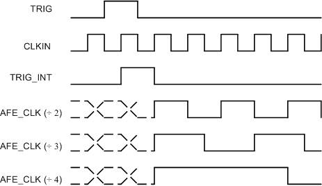 Figure 61. Input Clock Divider
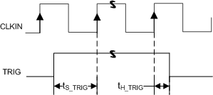 Figure 62. TRIG CLKIN Setup and Hold
Table 9. DIV_EN Register
| DIV_EN | DESCRIPTION |
|---|---|
| 0 | Divider disabled and bypassed |
| 1 | Divider enabled |
Table 10. DIV_FRC Register
| DIV_FRC | DESCRIPTION |
|---|---|
| 0 | Input divider ratio = serialization factor(1) (automatically set) |
| 1 | Input divider ratio = DIV_REG (manually set) |
Table 11. DIV_REG Register
| DIV_REG | DESCRIPTION |
|---|---|
| 0 | Divider disabled and bypassed |
| 1 | Divide-by-2 |
| 2 | Divide-by-3 |
| 3 | Divide-by-4 |
8.3.7 Data Output Serialization
The input signals are digitized by the dedicated channel ADCs. Digitized signals are multiplexed and output on D[11:0] as parallel data.
The output data rate and the DCLK speed are automatically calculated based on the CH_OUT_DIS[1:4] bits. The number of zeroes in these four bits is equal to the serialization factor for the output data. When the register bit is set to 1, the output for the respective channel is disabled. The channels are arranged in ascending order, with the lowest active channel output first and the highest active channel output last. CH_OUT_DIS[1:4] controls only the output serialization and does not power-down individual channels. Table 12 lists the register values with the respective serialization factors and output sequence.
Table 12. CH_OUT_DIS Register
| CH_OUT_DIS[1] | CH_OUT_DIS[2] | CH_OUT_DIS[3] | CH_OUT_DIS[4] | SERIALIZATION FACTOR | OUTPUT |
|---|---|---|---|---|---|
| 0 | 0 | 0 | 0 | 4 | CH1 → CH2 → CH3 → CH4 |
| 1 | 0 | 0 | 0 | 3 | CH2 → CH3 → CH4 |
| 0 | 1 | 0 | 0 | 3 | CH1 → CH3 → CH4 |
| 1 | 1 | 0 | 0 | 2 | CH3 → CH4 |
| 0 | 0 | 1 | 0 | 3 | CH1 → CH2 → CH4 |
| 1 | 0 | 1 | 0 | 2 | CH2 → CH4 |
| 0 | 1 | 1 | 0 | 2 | CH1 → CH4 |
| 1 | 1 | 1 | 0 | 1 | CH4 |
| 0 | 0 | 0 | 1 | 3 | CH1 → CH2 → CH3 |
| 1 | 0 | 0 | 1 | 2 | CH2 → CH3 |
| 0 | 1 | 0 | 1 | 2 | CH1 → CH3 |
| 1 | 1 | 0 | 1 | 1 | CH3 |
| 0 | 0 | 1 | 1 | 2 | CH1 → CH2 |
| 1 | 0 | 1 | 1 | 1 | CH2 |
| 0 | 1 | 1 | 1 | 1 | CH1 |
| 1 | 1 | 1 | 1 | 1 | Not supported |
8.3.8 Setting the Input Common-Mode Voltage for the Analog Inputs
8.3.8.1 Main Channels
The device analog input consists of a differential LNA. The common-mode for the LNA inputs is internally set using two internal, programmable, single-ended resistors, as shown in Figure 63.
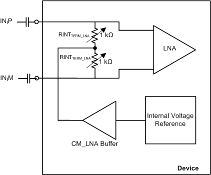 Figure 63. Common-Mode Biasing of LNA Input Pins
These resistors can be programmed to a higher value using the TERM_INT_20K_LNA register setting as described in Table 13.
Table 13. Internal Termination Register Setting (LNA)
| TERM_INT_20K_LNA | DESCRIPTION |
|---|---|
| 0 | RINTTERM_LNA = 1 kΩ |
| 1 | RINTTERM_LNA = 10 kΩ |
Hence, for proper operation, the input signal must be ac-coupled. Note that external input ac-coupling capacitors form a high-pass filter (HPF) with RINTTERM_LNA. Therefore, the capacitor values should allow the lowest frequency of interest to pass with minimum attenuation. For typical frequencies greater than 1 MHz, a value of 50 nF or greater is recommended. The maximum input swing is limited by the LNA gain setting. LNA output swing is limited to 2 VPP before the output becomes saturated or distorted.
Single ended mode of operation is also possible by connecting non-driven input pin to ground through a capacitor of 100 nF. However, this will result in reduced linearity.
8.3.8.2 Auxiliary Channel
The auxiliary analog inputs (INIP_AUX, INIM _AUX) can be enabled instead of the INIP, INIM inputs using the AUX_CHI_EN bits (Table 14). The auxiliary analog input signal path consists of an input unity-gain buffer followed by an ADC. The LNA, PGA, equalizer, and antialiasing filter are bypassed and powered down in this mode. Figure 64 shows the internal block diagram for auxiliary channel mode. When this mode is enabled, the maximum input swing is limited to 2 VPP before the input becomes saturated or distorted.
Table 14. AUX_CHI_EN Register
| AUX_CHI_EN | DESCRIPTION |
|---|---|
| 0 | INIP, INIM active, analog |
| 1 | INIP _AUX, INIM_AUX |
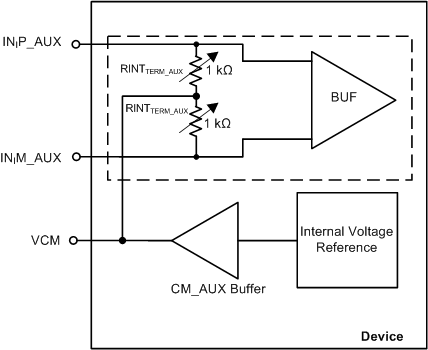
NOTE:
Dashed area denotes one of four channels.The dc common-mode on the INIP_AUX, INIM _AUX pins are internally biased to the optimum voltage (referred to as VCM).
The dc common-mode biasing is set with two internal, programmable, single-ended resistors (RINTTERM_AUX). These resistors can be programmed to a higher value using the TERM_INT_20K_AUX register setting as described in Table 15.
Table 15. Internal Termination Register Setting (AUX)
| TERM_INT_20K_AUX | DESCRIPTION |
|---|---|
| 0 | RINTTERM_AUX = 1 kΩ |
| 1 | RINTTERM_AUX = 10 kΩ |
The auxiliary inputs can also be ac-coupled as a result of the internal common-mode setting. The external input ac-coupling capacitors form a high-pass filter with RINTTERM_AUX. Therefore, the capacitor values should allow the lowest frequency of interest to pass with minimum attenuation.
For typical frequencies greater than 1 MHz, a value of 50 nF or greater is recommended. For instances where the input signal cannot be ac-coupled because of system requirements, it is recommended to use the VCM output to set the dc common-mode of the input signal. The driving capability of VCM is limited. A 100-nF capacitor should be connected on each VCM input to AVSS.
8.4 Device Functional Modes
8.4.1 Equalizer Mode
In some applications, the input signal power linearly decreases with signal frequency. Such types of input spectrum can be equalized using a first-order signal equalizer. The device can be configured in two different equalizer modes: EQ_EN and EQ_EN_LOW_FC. Table 16 lists the register settings for these modes.
- EQ_EN mode: In this mode, a high-pass filter (HPF) is added to the analog signal path between the LNA output and PGA input.
- EQ_EN_LOW_FC mode: In this mode, attenuation from the HPF is limited to unity in the pass-band frequency range.
Table 16. EQ_EN and EQ_EN_LOW_FC Registers
| EQ_EN | EQ_EN_LOW_FC | DESCRIPTION |
|---|---|---|
| 0 | 0 | Default mode |
| 0 | 1 | Default mode |
| 1 | 0 | Equalizer enabled |
| 1 | 1 | Equalizer with low-corner frequency enabled |
The HPF and LPF cutoff frequencies (of the antialiasing filter) are the same as per the FILTER_BW setting. In this mode, overall channel gain increases by an additional fixed gain of 15 dB from the HPF block. Typical frequency response plots showing different equalizer modes along with the default mode are shown in Figure 65 and Figure 66.
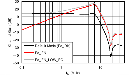 Figure 65. Filter Response (PGA Gain = 0 dB)
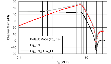 Figure 66. Filter Response (PGA Gain = 30 dB)
8.4.2 Data Output Mode
The functionality of DSYNC1, DSYNC2, DCLK, and D[11:0] are controlled by selecting the data output mode. The functionality of the DSYNC1, DSYNC2, DCLK, and D[11:0] output pins for 4x serialization modes are shown in Figure 67 and Figure 68. Any event on the TRIG pin triggers the DSYNC1 and DSYNC2 signals. The DSYNC1 period is determined by the COMP_DSYNC1 register value and the DSYNC2 period is determined by the SAMPLE_COUNT register value. When OUT_MODE_EN = 0, data output is continuous. When OUT_MODE_EN = 1, data is active only during the sample phase. Output pins are configured using the registers described in Table 17 through Table 21.
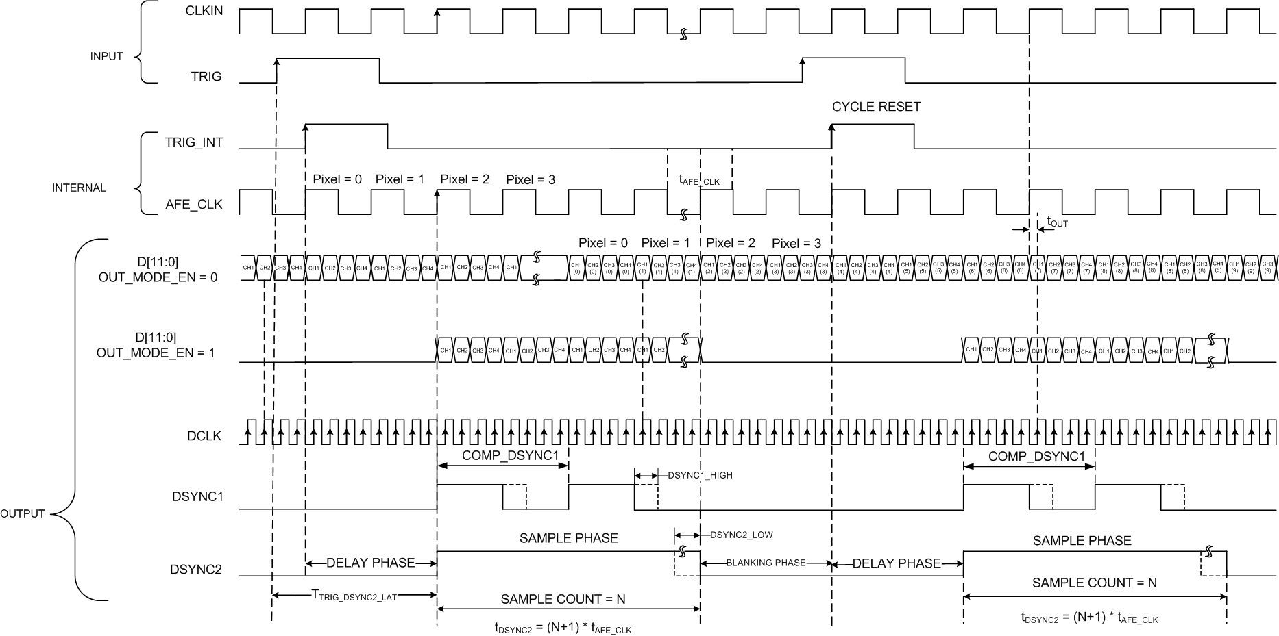 Figure 67. Data Output Timing Diagram (4x Serialization)
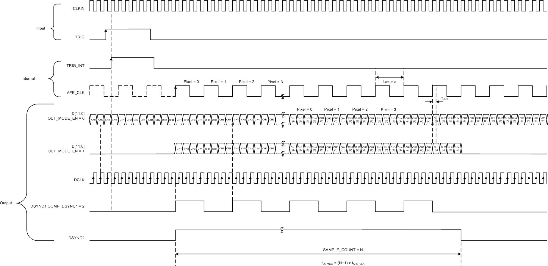 Figure 68. Data Output Timing Diagram (4x Serialization, Input Divider Enabled)
Table 17. Register Functions
| REGISTER | FUNCTION |
|---|---|
| DELAY_COUNT[23:0] | From a TRIG event, the sample phase is delayed for a DELAY_COUNT number of tAFE_CLK cycles |
| SAMPLE_COUNT[23:0] | From the end of DELAY_PHASE, the sample phase duration is the SAMPLE_COUNT number of tAFE_CLK cycles |
| COMP_DSYNC1[15:0] | DSYNC1 period in number of tAFE_CLKcycles |
Table 18. DSYNC1_START_LOW Register
| DSYNC1_START_LOW | DESCRIPTION |
|---|---|
| 0 | DSYNC1 is high at the sample phase start |
| 1 | DSYNC1 is low at the sample phase start |
Table 19. OUT_MODE_EN Register
| OUT_MODE_EN | DESCRIPTION |
|---|---|
| 0 | Data always active |
| 1 | Data active in sample phase |
Table 20. DSYNC_EN Register
| DSYNC_EN | DESCRIPTION |
|---|---|
| 0 | Disable DSYNC generation |
| 1 | Enable DSYNC generation |
Table 21. OUT_BLANK_HIZ Register
| OUT_BLANK_HIZ | DESCRIPTION |
|---|---|
| 0 | D[11:0] is low during inactive phase |
| 1 | D[11:0] is high impedance during inactive phase |
NOTE
The signal processing blocks in the device are always active and are not controlled by output mode configuration settings.
The functionality of the DSYNC1, DSYNC2, DCLK, and D[11:0] output pins with the input divider enabled for 3x serializations is shown in Figure 69.
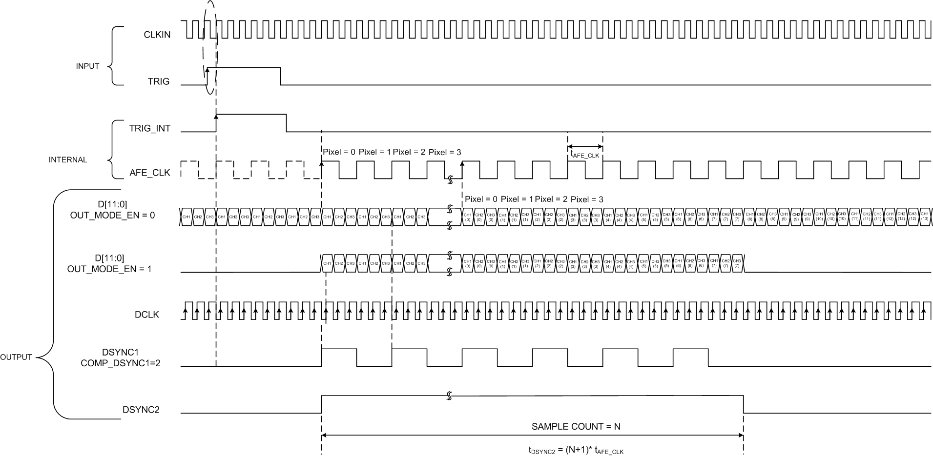 Figure 69. Data Output Timing (3x Serialization, Input Divider Enabled)
The TRIG to DSYNC2 latency is given by Table 22.
Table 22. TRIG to DSYNC2 Latency across Serialization Modes for AFE_CLK = 25 MHz
| Serialization Modes | TTRIG_DSYNC2_LAT(1) | Units |
|---|---|---|
| 4x | 230 | ns |
| 3x | 230 | ns |
| 2x | 240 | ns |
| 1x | 250 | ns |
8.4.2.1 Header
Each channel has an associated 12-bit header register. These registers can be written by an SPI write. The content of this register can be read out on the CMOS data output (D[11:0]) by configuring the HEADER_MODE register, as shown in Table 23.
Table 23. HEADER_MODE Register
| HEADER_MODE | DESCRIPTION |
|---|---|
| 0 | ADC data at output |
| 1 | Header data at output |
| 2 | [Temperature data, diagnostic data, mean, noise, (-1), (-1), (-1), (-1)]. This data sequence is repeated. |
| 3 | Header data, temperature data, diagnostic data, mean, noise, ADC data |
In HEADER_MODE = 3, the header mode data output is shown in Figure 70.
In this mode, header data is transmitted with a latency with respect to the TRIG input. This latency is given by Equation 2:
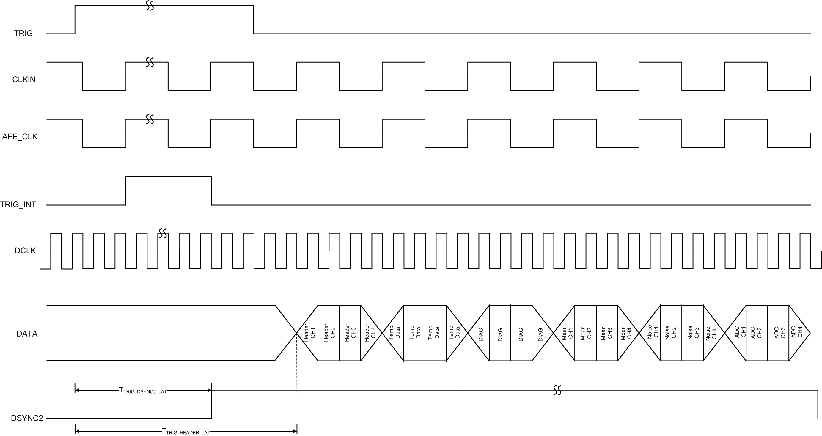 Figure 70. Header Mode Data Output (HEADER_MODE = 3)
8.4.2.2 Test Pattern Mode
In order to check the interface between the AFE and the receiver system, a test pattern can be directly programmed on the CMOS output. As shown in Table 24, different test patterns can be selected by setting the TST_PAT_MODE register.
Table 24. TST_PAT_MODE Register(1)
| TST_PAT_MODE | DESCRIPTION |
|---|---|
| 0 | Normal ADC output data |
| 1 | SYNC pattern (D[11:0] = 111111000000) |
| 2 | Deskew pattern (D[11:0] = 010101010101) |
| 3 | Custom pattern as per CUSTOM_PATTERN[11:0] register bits |
| 4 | All 1s |
| 5 | Toggle data (output toggles between all 0s and all 1s) |
| 6 | All 0s |
| 7 | Full-scale ramp data |
Similarly, in decimate-by-4 mode, three samples are dropped and thus output data D0 and D1 do not toggle for full-scale ramp data and output data D[11:0] does not toggle for toggle data.
8.4.3 Parity
Parity for each output sample of an active channel can be read on the D_GPO[1:0] pins by configuring these pins with the DGPO1_MODE, DGPO0_MODE register, as shown in Table 25. Parity generation can be enabled using the D_GPO_EN bit, as shown in Table 26. The type of parity generation can be configured to odd or even based on the PARITY_ODD bit, as shown in Table 27.
Table 25. DGPO0_MODE, DGPO1_MODE Register
| DGPO0_MODE, DGPO1_MODE | DESCRIPTION |
|---|---|
| 0 | Low |
| 1 | Parity |
| 2 | Overload |
| 3 | D[11] |
Table 26. D_GPO_EN Register
| D_GPO_EN | DESCRIPTION |
|---|---|
| 0 | D_GPO[x] pins are disabled |
| 1 | D_GPO[x] pins are enabled |
Table 27. PARITY_ODD Register
| PARITY_ODD | DESCRIPTION |
|---|---|
| 0 | Even |
| 1 | Odd |
8.4.4 Standby, Power-Down Mode
The device can be put into standby mode with the STDBY register bit. In this mode, all blocks except the ADC reference blocks are powered down. In GLOBAL_PDN mode, all blocks including the ADC reference blocks are powered down. However, in both modes, the serial interface is active.
8.4.5 Digital Filtering to Improve Stop-Band Attenuation
The device introduces a standard 11-tap, symmetric finite impulse response (FIR) digital filter for additional stop-band attenuation in decimate-by-2 and decimate-by-4 modes. In both modes, the FIR digital filter coefficients (C1 to C6) must be configured to obtain the desired filter characteristics. However, set 1 coefficients are loaded by default at device reset.
In this mode, device power consumption increases and the DSYNC period scales according to the decimation mode (the DSYNC period increases by 2x in decimate-by-2 mode and 4x in decimate-by-4 mode when compared to normal mode). Maximum AFE_CLK frequency supported in the decimation modes is 50 MHz.
8.4.5.1 Decimate-by-2 Mode
In this mode, the DECIMATE_2_EN and FILT_EN register bits must be set, and the filter coefficients should be configured. Figure 71 shows typical filter response in decimate-by-2 mode for the filter coefficient of set 1 (default). Note that the output data rate is reduced by a factor of 2 as compared to default mode for the given clock input frequency.
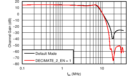 Figure 71. Decimate-by-2 Filter Response (fS = 50 MHz)
8.4.5.2 Decimate-by-4 Mode
In this mode, the DECIMATE_2_EN, DECIMATE_4_EN, and FILT_EN register bits must be set, and the filter coefficients should be configured. Figure 72 shows a typical filter response in decimate-by-4 mode for the filter coefficient of set 1 (default) and set 2. Note that the output data rate is reduced by a factor of 4 as compared to default mode for the given clock input frequency.
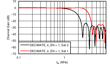
NOINDENT:
Set 1: C1 = 5, C2 = 2, C3 = –13, C4 = –2, C5 = 38, and C6 = 66. Set 2: C1 = –5, C2 = –2, C3 = 7, C4 = 19, C5 = 30, and C6 = 34.8.4.6 Diagnostic Mode
The device offers various diagnostic modes to check proper device operation at a system level. These modes can be enabled using the SPI and the outputs of these modes are stored in diagnostic read-only registers.
- Internal reference status check: In this mode, the on-chip band-gap voltage, ADC reference, and clock generation are verified for functionality. Reading a 0 on these bits indicates that these blocks are functioning properly. The DIAG_MODE_EN register bit must be set to 1. The DIG_REG register bits for this mode are:
- DIG_REG[0] for ADC references,
- DIG_REG[1] for band gap, and
- DIG_REG[2] for clock generation.
- DC input force: In this mode, a dc voltage can be internally forced at the LNA input to test the entire signal chain. During this test, the device analog inputs should be left floating. This mode can be asserted by setting the DC_INP_EN bit to 1 and programming the DC_INP_PROG[0:2] bits. In this mode, the equalizer is disabled internally.
- Variance (noise) and mean measurement: Variance and mean of the ADC output can be analyzed using the on-chip STAT module. The STAT_EN, STAT_CALC_CYCLE, and STAT_CH_SEL, STAT_CH_AUTO_SEL options should be set to compute the variance and mean. These values can be monitored using channel-specific, read-only registers. Alternatively, these values can also be read using HEADER_MODE. Output variance and mean calculation is determined by Equation 3.
- Temperature sensor: The device junction temperature measurement can be enabled and monitored using TEMP_SENS_EN and TEMP_CONV_EN. The temperature output is saved in a diagnostic read-only register, TEMP_DATA. Alternatively, this data can also be read using HEADER_MODE. The TEMP_DATA value is a 9-bit, twos complement data in degrees Celsius. The temperature data is internally updated as per Equation 4:
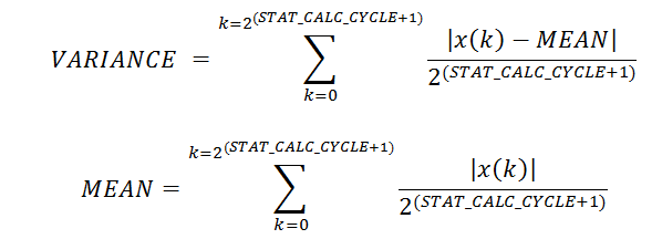
STAT_CALC_CYCLE must be set to a large value to obtain better accuracy. Mean provides the average dc value of the ADC output (mid code). The STAT module integration time is defined by: tAFE_CLK × 2(STAT_CALC_CYCLE+1) when the STAT_CH_SEL option is selected. When STAT_CH_AUTO_SEL is enabled, the STAT module integration time is defined by: 4 × tAFE_CLK × 2(STAT_CALC_CYCLE+1).
8.4.7 Signal Chain Probe
To enhance system-level debug capabilities, the device offers a mode where the output of each block in the signal chain can be connected to the ADC input. With this mode, internal signals can be easily monitored to ensure that each block output is not saturated. Figure 73 shows the device signal chain block diagram. Figure 74 and Figure 75 show typical frequency response plots at the output of each stage.
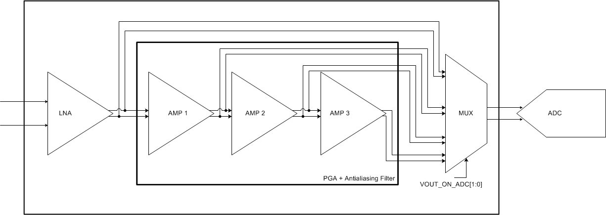 Figure 73. Signal Chain Block Diagram
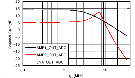 Figure 74. Frequency Response for
 VOUT_ON_ADC Settings (PGA Gain = 0 dB)
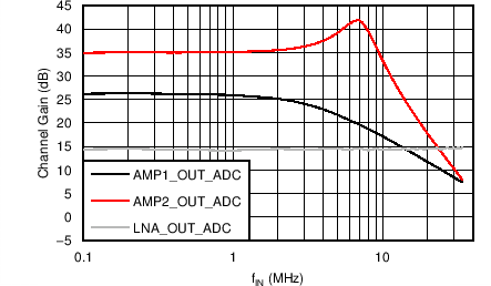 Figure 75. Frequency Response for
 VOUT_ON_ADC Settings (PGA Gain = 30 dB)
8.5 Programming
8.5.1 Serial Interface
Different modes can be programmed through the serial interface formed by the SEN (serial interface enable), SCLK (serial interface clock), SDATA (serial interface data) and RESET pins. SCLK and SDATA have a 150-kΩ pull-down resistor to ground and SEN has a 150-kΩ pull-up resistor to DVDD18. Serially shifting bits into the device is enabled when SEN is low. SDATA serial data bits are latched at every SCLK rising edge when SEN is active (low). Serial data bits are loaded into the register at every 24th SCLK rising edge when SEN is low. If the word length exceeds a multiple of 24 bits, the excess bits are ignored. Data bits can be loaded in multiples of 24-bit words within a single active SEN pulse (an internal counter counts groups of 24 clocks after the SEN falling edge). The interface can function with SCLK frequencies from 20 MHz down to very low speeds and even with a non-50% duty-cycle SCLK. Data bits are divided into two main portions: a register address (8 bits, A[7:0]) and data (16 bits, D[15:0]).
8.5.2 Register Initialization
After power up, the internal registers must be initialized to the default value (0). Initialization can be accomplished in one of two ways:
- Either through a hardware reset, by applying a positive pulse to the RESET pin, or
- Through a software reset with the serial interface, by setting the SW_RST bit high. Setting this bit initializes the internal registers to the respective default values (all 0s) and then self-resets the SW_RST bit low. In this case, the RESET pin can stay low (inactive).
NOTE
- No damage occurs to the part by applying voltage to the RESET pin while device power is off.
- For correct device operation, a positive pulse must be applied to the RESET pin. This pulse sets the internal control registers to 0. However, no power-supply sequencing is required.
- Reset only affects the digital registers and places the device in a default state. Reset does not function as a power-down and, therefore, all internal blocks are functional.
During a register write through the SPI, the effects on data propagate through the pipe while the internal registers change values. At the same time, some glitches may be present on the output because of the transition of register values (for instance, if any output-controlling modes change). The signal on the RESET pin must be low in order to write to the internal registers because reset is level-sensitive and asynchronous with the input clock. Although only 40 ns are required after the RESET rising edge to change the registers, the output data may take up to 20 clock cycles (worst-case) to be considered stable. For more information on RESET, see the Timing Requirements: RESET.
8.5.2.1 Register Write Mode
In register write mode, the REG_READ_EN bit must be set to 0. In this mode, the SDOUT signal outputs 0. Figure 76 shows this process.
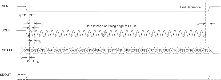 Figure 76. Serial Interface Register Write
8.5.2.2 Register Read Mode
In register readout mode, the REG_READ_EN bit must be set to 1. Then, a serial interface cycle should be initiated, specifying the address of the register (A[7:0]) whose content must be read out of the device. The data bits are don’t care. The device outputs the contents (D[15:0]) of the selected register on the SDOUT pin. The external controller latches the data on SDOUT at the SCLK rising edge. Figure 77 shows this process.
The timing specifications for the serial interface operation is listed in the Timing Requirements: Serial Interface Operation.
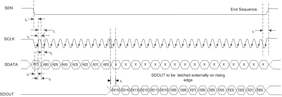 Figure 77. Serial Interface Register Readout Enable
8.5.3 CMOS Output Interface
The digital data from the four channels are multiplexed and output over a 12-bit parallel CMOS bus to reduce the device pin count. In addition to the data, a CMOS clock (DCLK) is also output, which can be used by the digital receiver to latch the AFE output data. The output data and clock buffers can typically drive a 5-pF load capacitance in default mode. To drive larger loads (10 pF to 15 pF), the strength of the CMOS output buffers can be increased using the STR_CTRL_CLK and STR_CTRL_DATA register bits. Note that the setup and hold time of the output data (with respect to DCLK) degrade with higher load capacitances. See Table 1, which provides timings for 5-pF and 15-pF load capacitances.
8.5.3.1 Synchronization and Triggering
While the digital data from the four channels is multiplexed on the output bus, some mechanism is required to identify the data from the individual channels. Other than the output data and DCLK, the device also outputs DSYNCx signals that can be used for channel identification.
The DSYNCx output signals function with the TRIG input signal. Every time that a trigger pulse is received on the TRIG pin, the device outputs the DSYNC1 and DSYNC2 signals. The DSYNCx signals can be configured in the following ways:
- The delay between the arrival of the TRIG signal and the DSYNCx signal becoming active is programmable in a number of AFE_CLK cycles (using the DELAY_COUNT register bit).
- The period of the DSYNC1 signal is programmable in terms of AFE_CLK clock cycles by using the COMP_DSYNC1 register bits.
- The active time of the DSYNC2 signal is programmable using the SAMPLE_COUNT register bits.
The rising edge of the DSYNC1 signal coincides with the channel 1 data, as shown in Figure 78. This occurrence can be used by the receiving device to identify individual channels.
The sample phase period corresponds to the period when valid data is available from the device when OUT_MODE_EN = 1.
 Figure 78. DSYNCx Timing Diagram
8.6 Register Maps
8.6.1 Functional Register Map
Table 28 shows the register map for the AFE5401 registers.
Table 28. Register Map
| REGISTER | BIT 15 | BIT 14 | BIT 13 | BIT 12 | BIT 11 | BIT 10 | BIT 9 | BIT 8 | BIT 7 | BIT 6 | BIT 5 | BIT 4 | BIT 3 | BIT 2 | BIT 1 | BIT 0 |
|---|---|---|---|---|---|---|---|---|---|---|---|---|---|---|---|---|
| 0 (00h) | 0 | 0 | 0 | 0 | 0 | 0 | 0 | 0 | 0 | 0 | 0 | 0 | 0 | 0 | REG_ READ_EN |
SW_RST |
| 1 (01h) | 0 | 0 | 0 | 0 | 0 | STDBY | 0 | 0 | DECIMATE _4_EN |
DIV_REG | DIV_FRC | DECIMATE _2_EN |
DIV_EN | SE_CLK_ MODE |
GLOBAL_ PDN |
|
| 2 (02h) | TST_PAT_MODE | 0 | 0 | 0 | 0 | 0 | 0 | DGPO0_MODE | DGPO1_MODE | 0 | 0 | 0 | ||||
| 3 (03h) | 0 | 0 | 0 | 0 | 0 | 0 | TEMP_DATA | |||||||||
| 4 (04h) | OUT_ BLANK_HIZ |
OUT_ MODE_EN |
DCLK_ INVERT |
TEMP_ CONV_EN |
TEMP_ SENS_EN |
0 | 0 | 0 | 0 | 0 | 0 | 0 | OFF_BIN_ DATA_FMT |
0 | 0 | 0 |
| 5 (05h) | CUSTOM_PAT | |||||||||||||||
| 6 (06h) | 0 | 0 | 0 | 0 | 0 | 0 | 0 | 0 | 0 | 0 | 0 | 0 | 0 | DIAG_REG | ||
| 7 (07h) | D_GPO_EN | PARITY_ ODD |
STAT_ EN | DCP_INP_ EN |
DCP_INP_PROG | DIAG_ MODE_EN |
0 | 0 | 0 | 0 | FILTER_BW | HEADER_MODE | ||||
| 8 (08h) | C2_FIR | DIG_GAIN_C1_FIR | ||||||||||||||
| 9 (09h) | C4_FIR | C3_FIR | ||||||||||||||
| 10 (0Ah) | C6_FIR | C5_FIR | ||||||||||||||
| 15 (0Fh) | 0 | 0 | 0 | 0 | 0 | FAST_ DGPO |
0 | 0 | 0 | 0 | 0 | 0 | 0 | 0 | 0 | 0 |
| 19 (13h) | 0 | OB_ DISABLE |
STR_CTRL_CLK | STR_CTRL_DATA | 0 | 0 | 0 | 0 | 0 | 0 | ||||||
| 21 (15h) | DELAY_COUNT[23:16] | SAMPLE_COUNT[23:16] | ||||||||||||||
| 22 (16h) | DELAY_COUNT[15:0] | |||||||||||||||
| 23 (17h) | SAMPLE_COUNT[15:0] | |||||||||||||||
| 24 (18h) | TRIG_FALL | DSYNC1_ START_ LOW |
0 | DSYNC_EN | 0 | COMP_DSYNC1[15:6] | 0 | |||||||||
| 25 (19h) | COMP_DSYNC1[5:0] | 0 | 0 | DSYNC2_LOW[23:16] | ||||||||||||
| 26 (1Ah) | DSYNC2_LOW[15:0] | |||||||||||||||
| 27 (1Bh) | DSYNC1_HIGH | |||||||||||||||
| 29 (1Dh) | OFFSET_ DIS |
0 | STAT_CH_SEL | 0 | 0 | STAT_CALC_CYCLE | 0 | 0 | 0 | 0 | STAT_CH_ AUTO_SEL |
|||||
| 30 (1Eh) | 0 | 0 | 0 | 0 | 0 | 0 | 0 | MULT_EN | FILT_EN | 0 | 0 | 0 | 0 | 0 | 0 | 0 |
| 32 (20h) | 0 | 0 | 0 | 0 | HEADER_CH1 | |||||||||||
| 33 (21h) | CH_OUT_ DIS1 |
AUX_CH1_EN | PDN_CH1 | INVERT_ CH1 |
0 | 0 | OFFSET_CH1 | |||||||||
| 34 (22h) | 0 | 0 | MEAN_CH1 | |||||||||||||
| 35 (23h) | 0 | 0 | NOISE_CH1 | |||||||||||||
| 36 (24h) | 0 | 0 | 0 | 0 | HEADER_CH2 | |||||||||||
| 37 (25h) | CH_OUT_ DIS2 |
AUX_CH2_EN | PDN_CH2 | INVERT_ CH2 |
0 | 0 | OFFSET_CH2 | |||||||||
| 38 (26h) | 0 | 0 | MEAN_CH2 | |||||||||||||
| 39 (27h) | 0 | 0 | NOISE_CH2 | |||||||||||||
| 40 (28h) | 0 | 0 | 0 | 0 | HEADER_CH3 | |||||||||||
| 41 (29h) | CH_OUT_ DIS3 |
AUX_CH3_EN | PDN_CH3 | INVERT_ CH3 |
0 | 0 | OFFSET_CH3 | |||||||||
| 42 (2A) | 0 | 0 | MEAN_CH3 | |||||||||||||
| 43(2B) | 0 | 0 | NOISE_CH3 | |||||||||||||
| 44 (2Ch) | 0 | 0 | 0 | 0 | HEADER_CH4 | |||||||||||
| 45 (2Dh) | CH_OUT_ DIS4 |
AUX_CH4_EN | PDN_CH4 | INVERT_ CH4 |
0 | 0 | OFFSET_CH4 | |||||||||
| 46(2Eh) | 0 | 0 | MEAN_CH4 | |||||||||||||
| 47(2Fh) | 0 | 0 | NOISE_CH4 | |||||||||||||
| 65 (41h) | 0 | 0 | 0 | 0 | 0 | TERM_INT_20K_AUX | 0 | 0 | 0 | 0 | 0 | 0 | 0 | 0 | 0 | 0 |
| 69 (45h) | TERM_INT_20K_LNA | LNA_GAIN | PGA_GAIN | EQ_EN | 0 | 0 | 0 | 0 | 0 | 0 | ||||||
| 70 (46h) | 0 | HPL_EN | 0 | 0 | 0 | 0 | 0 | 0 | 0 | 0 | 0 | 0 | 0 | 0 | VOUT_ON_ADC | |
| 71(47h) | 0 | 0 | 0 | 0 | 0 | 0 | 0 | 0 | 0 | 0 | 0 | 0 | HIGH_ POW_LNA |
EQ_ EN_LOW _FC |
0 | 0 |
| 100(64h) | 0 | HF_AFE_CLK_EN | 0 | 0 | 0 | 0 | 0 | 0 | 0 | 0 | 0 | 0 | 0 | 0 | 0 | |
8.6.2 Register Descriptions
| 15 | 14 | 13 | 12 | 11 | 10 | 9 | 8 |
| 0 | 0 | 0 | 0 | 0 | 0 | 0 | 0 |
| 7 | 6 | 5 | 4 | 3 | 2 | 1 | 0 |
| 0 | 0 | 0 | 0 | 0 | 0 | REG_READ_ EN |
SW_RST |
| Bits 15:2 | Must write 0 |
| Bit 1 | REG_READ_EN: Register read mode |
| 0 = Write (default) 1 = Enable register read |
|
| Bit 0 | SW_RST: Software reset |
| This bit is the software reset for the entire device. This bit is self-clearing. |
| 15 | 14 | 13 | 12 | 11 | 10 | 9 | 8 |
| 0 | 0 | 0 | 0 | 0 | STDBY | 0 | 0 |
| 7 | 6 | 5 | 4 | 3 | 2 | 1 | 0 |
| DECIMATE_4_EN | DIV_REG | DIV_FRC | DECIMATE_2_EN | DIV_EN | SE_CLK_ MODE |
GLOBAL_PDN | |
| Bits 15:11 | Must write 0 | |||
| Bit 10 | STDBY: Full device standby | |||
| 0 = Normal (default) 1 = Standby |
||||
| Bits 9:8 | Must write 0 | |||
| Bit 7 | DECIMATE_4_EN | |||
| 0 = Decimate-by-4 mode not enabled 1 = Decimate-by-4 mode enabled |
||||
| The DECIMATE_2_EN and FILT_EN bits must be set. FIR filter coefficients (C1 to C6) must be written for proper operation. If the AFE_CLK frequency > 25 MHz, then HF_AFE_CLK_EN must be set. |
||||
| Bits 6:5 | DIV_REG: Input clock divider ratio in DIV_FRC mode | |||
| DIV_REG | fAFE_CLK | |||
| 0 | CLKIN ÷ 1 | Input divider disabled and bypassed | ||
| 1 | CLKIN ÷ 2 | |||
| 2 | CLKIN ÷ 3 | |||
| 3 | CLKIN ÷ 4 | |||
| Bit 4 | DIV_FRC: Force input divider ratio | |||
| 0 = Auto computed based on CH_OUT_DISx (default). For more details, refer to Table 12. 1 = AFE clock frequency is based on DIV_REG settings |
||||
| Bit 3 | DECIMATE_2_EN | |||
| 0 = Normal mode 1 = Decimate-by-2 mode enabled |
||||
| The FILT_EN bit must be set for proper operation. FIR filter coefficients (C1 to C6) must be written for proper operation. If the AFE_CLK frequency > 25 MHz, then HF_AFE_CLK_EN must also be set. |
||||
| Bit 2 | DIV_EN: Enable CLKIN divider | |||
| 0 = Disabled and bypassed (default) 1 = Enabled |
||||
| Bit 1 | SE_CLK_MODE: Single-ended input clock configuration | |||
| 0 = Differential (default) 1 = Single-ended |
||||
| Bit 0 | GLOBAL_PDN: Full device power-down | |||
| 0 = Normal (default) 1 = Global PDN |
||||
| 15 | 14 | 13 | 12 | 11 | 10 | 9 | 8 |
| TST_PAT_MODE | 0 | 0 | 0 | 0 | 0 | ||
| 7 | 6 | 5 | 4 | 3 | 2 | 1 | 0 |
| 0 | DGPO0_MODE | DGPO1_MODE | 0 | 0 | 0 | ||
| Bits 15:13 | TST_PAT_MODE: Test pattern for CMOS output |
| 0 = Normal (default) 1 = SYNC 2 = Deskew 3 = Custom register 5[15:0] 4 = All 1s 5 = Toggle 6 = All 0s 7 = Ramp |
|
| Bits 12:7 | Must write 0 |
| Bits 6:5 | DGPO0_MODE: DGPO0 mode configuration |
| 0 = Low (default) 1 = Parity 2 = Overload 3 = D[11] |
|
| Bits 4:3 | DGPO1_MODE: DGPO1 mode configuration |
| 0 = Low (default) 1 = Parity 2 = Overload 3 = D[11] |
|
| Bits 2:0 | Must write 0 |
| 15 | 14 | 13 | 12 | 11 | 10 | 9 | 8 |
| 0 | 0 | 0 | 0 | 0 | 0 | TEMP_DATA | |
| 7 | 6 | 5 | 4 | 3 | 2 | 1 | 0 |
| TEMP_DATA | |||||||
| Bits 15:10 | Ignore bits |
| Bits 9:0 | TEMP_DATA: Read-only temperature readout register |
| Data is 9-bit, twos complement format in degrees Celsius. |
| 15 | 14 | 13 | 12 | 11 | 10 | 9 | 8 |
| OUT_BLANK_HIZ | OUT_MODE_ EN |
DCLK_INVERT | TEMP_CONV_EN | TEMP_SENS_EN | 0 | 0 | 0 |
| 7 | 6 | 5 | 4 | 3 | 2 | 1 | 0 |
| 0 | 0 | 0 | 0 | OFF_BIN_ DATA_FMT |
0 | 0 | 0 |
| Bit 15 | OUT_BLANK_HIZ: Output status during blanking phase |
| 0 = D[11:0] and D_GPO[1:0] are low (default) if EN_OUT_MODE = 1 1 = D[11:0] and D_GPO[1:0] are Hi-Z if EN_OUT_MODE = 1 |
|
| For more details, refer to Figure 67. | |
| Bit 14 | OUT_MODE_EN: Enables output mode gating with DSYNC2 |
| 0 = CMOS data is always active (default) 1 = Output mode enabled. Data is transmitted only during sample phase. |
|
| Bit 13 | DCLK_INVERT: Invert DCLK |
| 0 = DCLK rising edge at the center of data (default) 1 = DCLK falling edge at the center of data |
|
| Bit 12 | TEMP_CONV_EN: Enable Temperature Sensor output to digital conversion |
| 0 = Hold conversion 1 = Convert |
|
| Bit 11 | TEMP_SENS_EN: Enable temperature sensor block |
| 0 = Disable temperature sensor 1 = Enable temperature sensor |
|
| Bits 10:4 | Must write 0 |
| Bit 3 | OFF_BIN_DATA_FMT: Output data format |
| 0 = Twos complement (default) 1 = Offset binary |
|
| Bits 2:0 | Must write 0 |
| 15 | 14 | 13 | 12 | 11 | 10 | 9 | 8 |
| CUSTOM_PAT | |||||||
| 7 | 6 | 5 | 4 | 3 | 2 | 1 | 0 |
| CUSTOM_PAT | |||||||
| Bits 15:0 | CUSTOM_PAT: Custom pattern data |
| These bits set the custom data pattern. |
| 15 | 14 | 13 | 12 | 11 | 10 | 9 | 8 |
| 0 | 0 | 0 | 0 | 0 | 0 | 0 | 0 |
| 7 | 6 | 5 | 4 | 3 | 2 | 1 | 0 |
| 0 | 0 | 0 | 0 | 0 | DIAG_REG[2:0] | ||
| Bits 15:3 | Ignore bits |
| Bits 2:0 | DIAG_REG: Read only diagnostic readout register |
| DIAG_REG[0] = 0: ADC references are correct DIAG_REG[1] = 0: Indicates band gap is correct DIAG_REG[2] = 0: Indicates clock generation is correct |
| 15 | 14 | 13 | 12 | 11 | 10 | 9 | 8 |
| D_GPO_EN | PARITY_ODD | STAT_EN | DC_INP_EN | DC_INP_PROG | DIAG_MODE_EN | ||
| 7 | 6 | 5 | 4 | 3 | 2 | 1 | 0 |
| 0 | 0 | 0 | 0 | FILTER_BW | HEADER_MODE | ||
| Bit 15 | D_GPO_EN: Enable D_GPO functionality | |
| 0 = D_GPO[x] pins are disabled (default) 1 = D_GPO[x] pins are enabled |
||
| Bit 14 | PARITY_ODD: Parity type | |
| 0 = Even (default) 1 = Odd |
||
| Bit 13 | STAT_EN: Enable noise and mean calculation of ADC output | |
| 0 = Default 1 = Enables noise and mean computation if STAT_CALC_CYCLE is set. |
||
| Bit 12 | DC_INP_EN: Enable dc analog voltage at LNA input. In this mode, equalizer is disabled automatically. | |
| 0 = Normal 1 = DC input force is controlled by DC_INP_PROG. |
||
| Bits 11:9 | DC_INP_PROG: DC Input programmability | |
| 0 = 0 mV 1 = 0 mV 2 = 50 mV 3 = –50 mV |
4 = 100 mV 5 = –100 mV 6 = 100 mV 7 = –100 mV |
|
| Bit 8 | DIAG_MODE_EN: Enable diagnostic mode | |
| 0 = Disable diagnostic circuit 1 = Enable diagnostic circuit |
||
| Bits 7:4 | Must write 0 | |
| Bits 3:2 | FILTER_BW: Filter corner frequency | |
| 0 = 8 MHz (default) 1 = 7 MHz 2 = 10.5 MHz 3 = 12 MHz |
||
| Bits 1:0 | HEADER_MODE: Header output mode | |
| 0 = ADC data at output (default) 1 = Header data at output 2 = [Temperature data, diagnostic data, mean, noise, (-1), (-1), (-1), (-1)]. This data sequence is repeated. 3 = Header data, temperature data, diagnostic data, mean, noise, ADC data. Refer to Figure 70 for more information. |
||
| 15 | 14 | 13 | 12 | 11 | 10 | 9 | 8 |
| C2_FIR | |||||||
| 7 | 6 | 5 | 4 | 3 | 2 | 1 | 0 |
| DIG_GAIN_C1_FIR | |||||||
| Bits 15:8 | C2_FIR: Coefficient C2 for FIR digital filter (1) | |
| 2 = Default value | ||
| Bit 7:0 | DIG_GAIN_C1_FIR: Digital Gain common for all channels, coefficient C1 for decimation filter | |
|
Refer to Figure 60 for more information. |
||
| Mode | C1 Functionality | |
| With MULT_EN | DIG_GAIN | |
| With DECIMATE_X _EN | Coefficient C1 for FIR digital filter | |
| 5 = Default value | ||
| 15 | 14 | 13 | 12 | 11 | 10 | 9 | 8 |
| C4_FIR | |||||||
| 7 | 6 | 5 | 4 | 3 | 2 | 1 | 0 |
| C3_FIR | |||||||
| Bits 15:8 | C4_FIR: Coefficient C4 for FIR digital filter(1) |
| –2 = Default value | |
| Bit 7:0 | C3_FIR: Coefficient C3 for FIR digital filter(1) |
| –13 = Default value |
| 15 | 14 | 13 | 12 | 11 | 10 | 9 | 8 |
| C6_FIR | |||||||
| 7 | 6 | 5 | 4 | 3 | 2 | 1 | 0 |
| C5_FIR | |||||||
| Bits 15:8 | C6_FIR: Coefficient C6 for FIR digital filter(1) |
| 66 = Default value | |
| Bit 7:0 | C5_FIR: Coefficient C5 for FIR digital filter(1) |
| 38 = Default value |
| 15 | 14 | 13 | 12 | 11 | 10 | 9 | 8 |
| 0 | 0 | 0 | 0 | 0 | FAST_DGPO | 0 | 0 |
| 7 | 6 | 5 | 4 | 3 | 2 | 1 | 0 |
| 0 | 0 | 0 | 0 | 0 | 0 | 0 | 0 |
| Bits 15:11, and Bits 9:0 |
Must write 0 |
| Bit 10 | FAST_DGPO: Fast DGPO output buffer |
| 0 = Default strength (default) 1 = Higher drive strength on D_GPO[x] pins. |
|
| Must write 0 |
| 15 | 14 | 13 | 12 | 11 | 10 | 9 | 8 |
| 0 | OB_DISABLE | STR_CTRL_CLK | STR_CTRL_DATA | ||||
| 7 | 6 | 5 | 4 | 3 | 2 | 1 | 0 |
| STR_CTRL_DATA | 0 | 0 | 0 | 0 | 0 | 0 | |
| Bits 15, Bits 5:0 | Must write 0 | |||
| Bit 14 | OB_DISABLE: CMOS output buffers D[11:0], DCLK disabled | |||
| 0 = Active CMOS output buffers 1 = Hi-Z CMOS output Buffers |
||||
| Bits 13:10 | STR_CTRL_CLK: Controls strength of CMOS output DCLK buffer | |||
| STR_CTRL_CLK | Drive Strength | DRVDD (V) | ||
| 0 | Default strength (CLOAD = 5 pF) | 3.3 | ||
| 6 | Maximum strength (CLOAD = 15 pF) | 3.3 | ||
| 5 | Default strength (CLOAD = 5 pF) | 1.8 | ||
| 14 | Maximum strength (CLOAD = 15 pF) | 1.8 | ||
| All other options are reserved. | ||||
| Bit 9:6 | STR_CTRL_DATA: Controls strength of CMOS output DATA buffers | |||
| STR_CTRL_DATA | Drive Strength | DRVDD (V) | ||
| 0 | Default strength (CLOAD = 5 pF) | 3.3 | ||
| 6 | Maximum strength (CLOAD = 15 pF) | 3.3 | ||
| 5 | Default strength (CLOAD = 5 pF) | 1.8 | ||
| 14 | Maximum strength (CLOAD = 15 pF) | 1.8 | ||
| All other options are reserved. | ||||
| 15 | 14 | 13 | 12 | 11 | 10 | 9 | 8 |
| DELAY_COUNT[23:16] | |||||||
| 7 | 6 | 5 | 4 | 3 | 2 | 1 | 0 |
| SAMPLE_COUNT[23:16] | |||||||
| Bits 15:8 | DELAY_COUNT[23:16]: Delay counter, upper bits |
| These bits determine the delay phase in terms of tAFE_CLK. | |
| DELAY_PHASE = (DELAY_COUNT + 1) × tAFE_CLK. The valid range for DELAY_COUNT is from 0 to (224 – 2). The maximum supported values of DELAY_COUNT + SAMPLE_COUNT is (224 – 2). |
|
| Bits 7:0 | SAMPLE_COUNT[23:16]: Sample counter, upper bits |
| These bits determine the sample phase in terms of tAFE_CLK. | |
| Sample phase = (SAMPLE_COUNT + 1) × tAFE_CLK. The valid range for SAMPLE_COUNT is from 0 to (224 – 2). The maximum supported values of DELAY_COUNT + SAMPLE_COUNT is (224 – 2). |
| 15 | 14 | 13 | 12 | 11 | 10 | 9 | 8 |
| DELAY_COUNT[15:0] | |||||||
| 7 | 6 | 5 | 4 | 3 | 2 | 1 | 0 |
| DELAY_COUNT[15:0] | |||||||
| Bits 15:0 | DELAY_COUNT[15:0]: Delay counter, lower bits |
| These bits determine the delay phase in terms of tAFE_CLK. | |
| DELAY_PHASE = (DELAY_COUNT + 1) × tAFE_CLK. The valid range for DELAY_COUNT is from 0 to (224 – 2). The maximum supported values of DELAY_COUNT + SAMPLE_COUNT is (224 – 2). |
| 15 | 14 | 13 | 12 | 11 | 10 | 9 | 8 |
| SAMPLE_COUNT[15:0] | |||||||
| 7 | 6 | 5 | 4 | 3 | 2 | 1 | 0 |
| SAMPLE_COUNT[15:0] | |||||||
| Bits 15:0 | SAMPLE_COUNT[15:0]: Sample counter, lower bits |
| These bits determine the sample phase in terms of tAFE_CLK. | |
| Sample phase = (SAMPLE_COUNT + 1) × tAFE_CLK. The valid range for SAMPLE_COUNT is from 0 to (224 – 2). The maximum supported values of DELAY_COUNT + SAMPLE_COUNT is (224 – 2). |
| 15 | 14 | 13 | 12 | 11 | 10 | 9 | 8 |
| TRIG_FALL | DSYNC1_ START_LOW |
0 | DSYNC_EN | 0 | COMP_DSYNC1[15:6] | ||
| 7 | 6 | 5 | 4 | 3 | 2 | 1 | 0 |
| COMP_DSYNC1[15:6] | 0 | ||||||
| Bit 15 | TRIG_FALL |
| 0 = TRIG event on the TRIG rising edge 1 = TRIG event on the TRIG falling edge |
|
| Bit 14 | DSYNC1_START_LOW: Selects DSYNC1 start level |
| 0 = DSYNC1 starts with logic high (default) 1 = DSYNC1 starts with logic low |
|
| Bit 13 | Must write 0 |
| Bit 12 | DSYNC_EN: Enable DSYNC1/2 generation |
| 0 = Disable DSYNC1/2 signals (default - logic low) 1 = Enable DSYNC1/2 signals |
|
| Bit 11 | Must write 0 |
| Bits 10:1 | COMP_DSYNC1[15:6]: DSYNC1, upper bits |
| These bits determine the DSYNC1 period in the number of tAFE_CLK cycles. For COMP_DSYNC1 = 0 or 1, DSYNC1 is static. | |
| Bit 0 | Must write 0 |
| 15 | 14 | 13 | 12 | 11 | 10 | 9 | 8 |
| COMP_DSYNC1[5:0] | 0 | 0 | |||||
| 7 | 6 | 5 | 4 | 3 | 2 | 1 | 0 |
| DSYNC2_LOW[23:16] | |||||||
| Bits 15:10 | COMP_DSYNC1[5:0]: DSYNC1, lower bits |
| These bits determine the DSYNC1 period in the number of tAFE_CLK cycles. For COMP_DSYNC1 = 0 or 1, DSYNC1 is static. | |
| Bits 9:8 | Must write 0 |
| Bits 7:0 | DSYNC2_LOW[23:16]: DSYNC2, upper bits |
| Low pulse duration of DSYNC2 in number of tAFE_CLK clocks. |
| 15 | 14 | 13 | 12 | 11 | 10 | 9 | 8 |
| DSYNC2_LOW[15:0] | |||||||
| 7 | 6 | 5 | 4 | 3 | 2 | 1 | 0 |
| DSYNC2_LOW[15:0] | |||||||
| Bits 15:0 | DSYNC2_LOW[15:0]: DSYNC2, lower bits |
| Low pulse duration of DSYNC2 in number of tAFE_CLK clocks. |
| 15 | 14 | 13 | 12 | 11 | 10 | 9 | 8 |
| DSYNC1_HIGH | |||||||
| 7 | 6 | 5 | 4 | 3 | 2 | 1 | 0 |
| DSYNC1_HIGH | |||||||
| Bits 15:0 | DSYNC1_HIGH: DSYNC1 |
| High pulse duration of DSYNC1, in number of tAFE_CLK clocks. | |
| DSYNC1 high = high for [(DSYNC1_HI + COMP_DSYNC1 ÷ 2) Mod (1) COMP_DSYNC1] |
| 15 | 14 | 13 | 12 | 11 | 10 | 9 | 8 |
| OFFSET_DIS | 0 | STAT_CH_SEL | 0 | 0 | STAT_CALC_CYCLE | ||
| 7 | 6 | 5 | 4 | 3 | 2 | 1 | 0 |
| STAT_CALC_CYCLE | 0 | 0 | 0 | 0 | STAT_CH_AUTO_SEL | ||
| Bit 15 | OFFSET_DIS: Bypass OFFSET addition at channel output |
| 0 = Default. The OFFSET_CHx register value is added to the channel output. 1 = Disable OFFSET. The OFFSET_CHx register value is not added to the channel output. |
|
| Bit 14 | Always write 0 |
| Bits 13:12 | STAT_CH_SEL: Manual channel selection for computation by STAT module |
| 0 = Channel 1 1 = Channel 2 2 = Channel 3 3 = Channel 4 |
|
| Bits 11:10 | Always write 0 |
| Bits 9:5 | STAT_CALC_CYCLE |
| Number of ADC samples used for STAT computation = 2STAT_CALC_CYCLE+1, STAT_CALC_CYCLE range = 0 to 30 | |
| and Bits 4:1 | Always write 0 |
| Bit 0 | STAT_CH_AUTO_SEL: Automatic channel selection for SNR Computation |
| 0 = Static, computation is done based on the STAT_CH_SEL selection 1 = Auto, computation is sequentially done for all four channels |
| 15 | 14 | 13 | 12 | 11 | 10 | 9 | 8 |
| 0 | 0 | 0 | 0 | 0 | 0 | 0 | MULT_EN |
| 7 | 6 | 5 | 4 | 3 | 2 | 1 | 0 |
| FILT_EN | 0 | 0 | 0 | 0 | 0 | 0 | 0 |
| Bits 15:9 | Must write 0 |
| Bit 8 | MULT_EN: Channel multiplier enable |
| 0 = Disable multiplier 1 = Enable multiplier. For digital gain, DIG_GAIN_C1_FIR must be written. |
|
| Bit 7 | FILT_EN: Digital decimation filter enable |
| 0 = Disable filter 1 = Enable standard 11-tap, symmetric FIR digital filter. |
|
| Bits 6:0 | Must write 0 |
| 15 | 14 | 13 | 12 | 11 | 10 | 9 | 8 |
| 0 | 0 | 0 | 0 | HEADER_CH1 | |||
| 7 | 6 | 5 | 4 | 3 | 2 | 1 | 0 |
| HEADER_CH1 | |||||||
| Bits 15:12 | Must write 0 |
| Bits 11:0 | HEADER_CH1: Header information for channel 1 |
| These bits provide the header information for channel 1. |
| 15 | 14 | 13 | 12 | 11 | 10 | 9 | 8 |
| CH_OUT_DIS1 | AUX_CH1_EN | PDN_CH1 | INVERT_ CH1 | 0 | 0 | OFFSET_CH1 | |
| 7 | 6 | 5 | 4 | 3 | 2 | 1 | 0 |
| OFFSET_CH1 | |||||||
| Bit 15 | CH_OUT_DIS1: Channel 1 disable |
| Channel 1 is not muxed out. | |
| 0 = Channel 1 is output (default) 1 = Channel 1 is not output |
|
| Bit 14 | AUX_CH1_EN: Enable auxiliary channel for channel 1 |
| 0 = Filter (default) 1 = Auxiliary |
|
| Bit 13 | PDN_CH1: Power-down channel 1 |
| 0 = Active (default) 1 = Power-down |
|
| Bit 12 | INVERT_CH1: Invert channel 1 output |
| 0 = Normal ouput (default) 1 = Inverted output |
|
| Bits 11:10 | Must write 0 |
| Bits 9:0 | OFFSET_CH1: Output offset of channel 1 range |
| Output offset value = OFFSET_CH1 ÷ 4, output offset value is added to channel output. |
| 15 | 14 | 13 | 12 | 11 | 10 | 9 | 8 |
| 0 | 0 | MEAN_CH1 | |||||
| 7 | 6 | 5 | 4 | 3 | 2 | 1 | 0 |
| MEAN_CH1 | |||||||
| Bits 15:14 | Must write 0 |
| Bits 13:0 | MEAN_CH1: Mean for channel 1 (read-only register) |
| These bits provide the mean information computed by STAT module for channel 1. |
| 15 | 14 | 13 | 12 | 11 | 10 | 9 | 8 |
| 0 | 0 | NOISE_CH1 | |||||
| 7 | 6 | 5 | 4 | 3 | 2 | 1 | 0 |
| NOISE_CH1 | |||||||
| Bits 15:14 | Must write 0 |
| Bits 13:0 | NOISE_CH1: Noise for channel 1 (read-only register) |
| These bits provide the noise information computed by STAT module for channel 1. |
| 15 | 14 | 13 | 12 | 11 | 10 | 9 | 8 |
| 0 | 0 | 0 | 0 | HEADER_CH2 | |||
| 7 | 6 | 5 | 4 | 3 | 2 | 1 | 0 |
| HEADER_CH2 | |||||||
| Bits 15:12 | Must write 0 |
| Bits 11:0 | HEADER_CH2: Header information for channel 2 |
| These bits provide the header information for channel 2. |
| 15 | 14 | 13 | 12 | 11 | 10 | 9 | 8 |
| CH_OUT_DIS2 | AUX_CH2_EN | PDN_CH2 | INVERT_CH2 | 0 | 0 | OFFSET_CH2 | |
| 7 | 6 | 5 | 4 | 3 | 2 | 1 | 0 |
| OFFSET_CH2 | |||||||
| Bit 15 | CH_OUT_DIS2: Channel 2 disable |
| Channel 2 is not muxed out. | |
| 0 = Channel 2 is output (default) 1 = Channel 2 is not output |
|
| Bit 14 | AUX_CH2_EN: Enable auxiliary channel for channel 2 |
| 0 = Filter (default) 1 = Auxiliary |
|
| Bit 13 | PDN_CH2: Power-down channel 2 |
| 0 = Active (default) 1 = Power-down |
|
| Bit 12 | INVERT_CH2: Invert channel 2 output |
| 0 = Normal (default) 1 = Inverted output |
|
| Bits 11:10 | Must write 0 |
| Bits 9:0 | OFFSET_CH2: Output offset of Channel 2 |
| Output offset value = OFFSET_CH2 ÷ 4, output offset value is added to the channel output |
| 15 | 14 | 13 | 12 | 11 | 10 | 9 | 8 |
| 0 | 0 | MEAN_CH2 | |||||
| 7 | 6 | 5 | 4 | 3 | 2 | 1 | 0 |
| MEAN_CH2 | |||||||
| Bits 15:14 | Must write 0 |
| Bits 13:0 | MEAN_CH2: Mean for channel 2 (read-only register) |
| These bits provide the mean information computed by the STAT module for channel 2. |
| 15 | 14 | 13 | 12 | 11 | 10 | 9 | 8 |
| 0 | 0 | NOISE_CH2 | |||||
| 7 | 6 | 5 | 4 | 3 | 2 | 1 | 0 |
| NOISE_CH2 | |||||||
| Bits 15:14 | Must write 0 |
| Bits 13:0 | NOISE_CH2: Noise for channel 2 (read-only register) |
| These bits provide the noise information computed by the STAT module for channel 2. |
| 15 | 14 | 13 | 12 | 11 | 10 | 9 | 8 |
| 0 | 0 | 0 | 0 | HEADER_CH3 | |||
| 7 | 6 | 5 | 4 | 3 | 2 | 1 | 0 |
| HEADER_CH3 | |||||||
| Bits 15:12 | Must write 0 |
| Bits 11:0 | HEADER_CH3: Header information for channel 3 |
| These bits provide the header information for channel 3. |
| 15 | 14 | 13 | 12 | 11 | 10 | 9 | 8 |
| CH_OUT_DIS3 | AUX_CH3_EN | PDN_CH3 | INVERT_CH3 | 0 | 0 | OFFSET_CH3 | |
| 7 | 6 | 5 | 4 | 3 | 2 | 1 | 0 |
| OFFSET_CH3 | |||||||
| Bit 15 | CH_OUT_DIS3: Channel 3 disable |
| Channel 3 is not muxed out. | |
| 0 = Channel 3 is output (default) 1 = Channel 3 is not output |
|
| Bit 14 | AUX_CH3_EN: Enable auxiliary channel for channel 3 |
| 0 = Filter (default) 1 = Auxiliary |
|
| Bit 13 | PDN_CH3: Power-down channel 3 |
| 0 = Active (default) 1 = Power-down |
|
| Bit 12 | INVERT_CH3: Invert channel 3 output |
| 0 = Normal (default) 1 = Inverted output |
|
| Bits 11:10 | Must write 0 |
| Bits 9:0 | OFFSET_CH3: Output offset of Channel 3 |
| Output offset value = OFFSET_CH3 ÷ 4, output offset value is added to the channel output |
| 15 | 14 | 13 | 12 | 11 | 10 | 9 | 8 |
| 0 | 0 | MEAN_CH3 | |||||
| 7 | 6 | 5 | 4 | 3 | 2 | 1 | 0 |
| MEAN_CH3 | |||||||
| Bits 15:14 | Must write 0 |
| Bits 13:0 | MEAN_CH3: Mean for channel 3 (read-only register) |
| These bits provide the mean information computed by the STAT module for channel 3. |
| 15 | 14 | 13 | 12 | 11 | 10 | 9 | 8 |
| 0 | 0 | NOISE_CH3 | |||||
| 7 | 6 | 5 | 4 | 3 | 2 | 1 | 0 |
| NOISE_CH3 | |||||||
| Bits 15:14 | Must write 0 |
| Bits 13:0 | NOISE_CH3: Noise for channel 3 (read-only register) |
| These bits provide the noise information computed by the STAT module for channel 3. |
| 15 | 14 | 13 | 12 | 11 | 10 | 9 | 8 |
| 0 | 0 | 0 | 0 | HEADER_CH4 | |||
| 7 | 6 | 5 | 4 | 3 | 2 | 1 | 0 |
| HEADER_CH4 | |||||||
| Bits 15:12 | Must write 0 |
| Bits 11:0 | HEADER_CH4: Header information for channel 4 |
| These bits provide the header information for channel 4. |
| 15 | 14 | 13 | 12 | 11 | 10 | 9 | 8 |
| CH_OUT_DIS4 | AUX_CH4_EN | PDN_CH4 | INVERT_CH4 | 0 | 0 | OFFSET_CH4 | |
| 7 | 6 | 5 | 4 | 3 | 2 | 1 | 0 |
| OFFSET_CH4 | |||||||
| Bit 15 | CH_OUT_DIS1: Channel 4 disable |
| Channel 4 is not muxed out. | |
| 0 = Channel 4 is output (default) 1 = Channel 4 is not output |
|
| Bit 14 | AUX_CH4_EN: Enable auxiliary channel for channel 4 |
| 0 = Filter (default) 1 = Auxiliary |
|
| Bit 13 | PDN_CH4: Power-down channel 4 |
| 0 = Active (default) 1 = Power-down |
|
| Bit 12 | INVERT_CH4: Invert channel 4 output |
| 0 = Normal (default) 1 = Inverted output |
|
| Bits 11:10 | Must write 0 |
| Bits 9:0 | OFFSET_CH4: Output offset of channel 4 |
| Output offset value = OFFSET_CH4 ÷ 4, output offset value is added to the channel output |
| 15 | 14 | 13 | 12 | 11 | 10 | 9 | 8 |
| 0 | 0 | MEAN_CH4 | |||||
| 7 | 6 | 5 | 4 | 3 | 2 | 1 | 0 |
| MEAN_CH4 | |||||||
| Bits 15:14 | Must write 0 |
| Bits 13:0 | MEAN_CH4: Mean for channel 4 (read-only register) |
| These bits provide the mean information computed by the STAT module for channel 4. |
| 15 | 14 | 13 | 12 | 11 | 10 | 9 | 8 |
| 0 | 0 | NOISE_CH4 | |||||
| 7 | 6 | 5 | 4 | 3 | 2 | 1 | 0 |
| NOISE_CH4 | |||||||
| Bits 15:14 | Must write 0 |
| Bits 13:0 | NOISE_CH4: Noise for channel 4 (read-only register) |
| These bits provide the noise information computed by the STAT module for channel 4. |
| 15 | 14 | 13 | 12 | 11 | 10 | 9 | 8 |
| 0 | 0 | 0 | 0 | 0 | TERM_INT_ 20K_AUX |
0 | 0 |
| 7 | 6 | 5 | 4 | 3 | 2 | 1 | 0 |
| 0 | 0 | 0 | 0 | 0 | 0 | 0 | 0 |
| Bits 15:11 | Must write 0 |
| Bit 10 | TERM_INT_20K_AUX: Auxiliary input termination |
| This bit is common for all channels. This bit provides an auxiliary input internal differential termination of 20 kΩ. | |
| 0 = 2-kΩ differential resistance (default) 1 = 20-kΩ differential resistance |
|
| Bits 9:0 | Must write 0 |
| 15 | 14 | 13 | 12 | 11 | 10 | 9 | 8 |
| TERM_INT_ 20K_LNA |
LNA_GAIN | PGA_GAIN | |||||
| 7 | 6 | 5 | 4 | 3 | 2 | 1 | 0 |
| PGA_GAIN | EQ_EN | 0 | 0 | 0 | 0 | 0 | 0 |
| Bit 15 | TERM_INT_20K_LNA: LNA input termination | |
| This bit is common for all channels. This bit provides LNA input internal differential termination of 20 kΩ. | ||
| 0 = 2-kΩ differential resistance (default) 1 = 20-kΩ differential resistance |
||
| Bits 14:13 | LNA_GAIN: LNA gain | |
| These bits are common for all channels. | ||
| 0 = 15 dB (default) 1 = 18 dB 2 = 12 dB 3 = 16.5 dB |
||
| Bits 12:7 | PGA_GAIN: PGA gain | |
| These bits are common for all channels. PGA gain = 0 dB, 3 dB, 6 dB, 9 dB, 12 dB, 15 dB, 18 dB, 21 dB, 24 dB, 27 dB, and 30 dB. | ||
| 0 = 0 dB 1 = 3 dB 2 = 6 dB 3 = 9 dB 4 = 12 dB 5 = 15 dB |
6 = 18 dB 7 = 21 dB 8 = 24 dB 9 = 27 dB 10 = 30 dB |
|
| Bit 6 | EQ_EN: Equalizer enable | |
| These bits are common for all channels. | ||
| 0 = Disabled (default) 1 = Enabled |
||
| Bits 5:0 | Must write 0 | |
| 15 | 14 | 13 | 12 | 11 | 10 | 9 | 8 |
| 0 | HPL_EN | 0 | 0 | 0 | 0 | 0 | 0 |
| 7 | 6 | 5 | 4 | 3 | 2 | 1 | 0 |
| 0 | 0 | 0 | 0 | 0 | 0 | VOUT_ON_ADC | |
| Bit 15 | Must write 0 |
| Bit 14 | HPL_EN: High-performance linearity mode |
| 0 = Default 1 = Improves linearity (HD3) with increased power dissipation |
|
| Bits 13:2 | Must write 0 |
| Bits 1:0 | VOUT_ON_ADC: Check analog block output on ADC input |
| 0 = LNA + antialiasing filter + ADC (default) 1 = LNA + ADC 2 = AMP1 + ADC 3 = AMP2 + ADC |
| 15 | 14 | 13 | 12 | 11 | 10 | 9 | 8 |
| 0 | 0 | 0 | 0 | 0 | 0 | 0 | 0 |
| 7 | 6 | 5 | 4 | 3 | 2 | 1 | 0 |
| 0 | 0 | 0 | 0 | HIGH_POW_ LNA |
EQ_EN_LOW_ FC |
0 | 0 |
| Bits 15:4 | Must write 0 |
| Bit 3 | HIGH_POW_LNA |
| 0 = Default mode 1 = High-power LNA improves channel input-referred noise at high LNA and PGA gains compared to default mode. This mode increases power dissipation. |
|
| Bit 2 | EQ_EN_LOW_FC: Enable Equalizer Low Frequency Corner Frequency |
| 0 = Disable 1 = Enable; EQ_EN must also be enabled for this mode |
|
| Bits 1:0 | Must write 0 |
| 15 | 14 | 13 | 12 | 11 | 10 | 9 | 8 |
| 0 | HF_AFE_CLK_EN | 0 | 0 | 0 | 0 | 0 | |
| 7 | 6 | 5 | 4 | 3 | 2 | 1 | 0 |
| 0 | 0 | 0 | 0 | 0 | 0 | 0 | 0 |
| Bits 15 | Must write 0 |
| Bits 14:13 | HF_AFE_CLK_EN |
| 0 = Default 3 = For fAFE_CLK > 25 MHz ( in decimation modes) |
|
| Bits 12:0 | Must write 0 |
