ZHCSDZ6D July 2012 – July 2015 DS90UB913Q-Q1 , DS90UB914Q-Q1
PRODUCTION DATA.
- 1 特性
- 2 应用
- 3 说明
- 4 修订历史记录
- 5 说明(续)
- 6 器件比较表
- 7 Pin Configuration and Functions
-
8 Specifications
- 8.1 Absolute Maximum Ratings
- 8.2 ESD Ratings
- 8.3 Recommended Operating Conditions
- 8.4 Thermal Information
- 8.5 Electrical Characteristics
- 8.6 Timing Requirements: Recommended for Serializer PCLK
- 8.7 AC Timing Specifications (SCL, SDA) - I2C Compliant
- 8.8 Bidirectional Control Bus DC Timing Specifications (SCL, SDA) - I2C Compliant
- 8.9 Switching Characteristics: Serializer
- 8.10 Switching Characteristics: Deserializer
- 8.11 Typical Characteristics
- 9 Parameter Measurement Information
-
10Detailed Description
- 10.1 Overview
- 10.2 Functional Block Diagram
- 10.3
Feature Description
- 10.3.1 Serial Frame Format
- 10.3.2 Line Rate Calculations for the DS90UB91xQ
- 10.3.3 Deserializer Multiplexer Input
- 10.3.4 Error Detection
- 10.3.5 Description of Bidirectional Control Bus and I2C Modes
- 10.3.6 Slave Clock Stretching
- 10.3.7 I2C Pass-Through
- 10.3.8 ID[x] Address Decoder on the Serializer
- 10.3.9 ID[x] Address Decoder on the Deserializer
- 10.3.10 Programmable Controller
- 10.3.11 Synchronizing Multiple Cameras
- 10.3.12 General-Purpose I/O (GPIO) Descriptions
- 10.3.13 LVCMOS VDDIO Option
- 10.3.14 Deserializer - Adaptive Input Equalization (AEQ)
- 10.3.15 EMI Reduction
- 10.4
Device Functional Modes
- 10.4.1 DS90UB91xQ-Q1 Operation With External Oscillator as Reference Clock
- 10.4.2 DS90UB91xQ-Q1 Operation With Pixel Clock from Imager as Reference Clock
- 10.4.3 MODE Pin on Serializer
- 10.4.4 MODE Pin on Deserializer
- 10.4.5 Clock-Data Recovery Status Flag (LOCK), Output Enable (OEN) and Output State Select (OSS_SEL)
- 10.4.6 Multiple Device Addressing
- 10.4.7 Powerdown
- 10.4.8 Pixel Clock Edge Select (TRFB / RRFB)
- 10.4.9 Power-Up Requirements and PDB Pin
- 10.4.10 Built-In Self Test
- 10.4.11 BIST Configuration and Status
- 10.5 Register Maps
- 11Application and Implementation
- 12Power Supply Recommendations
- 13Layout
- 14器件和文档支持
- 15机械、封装和可订购信息
10 Detailed Description
10.1 Overview
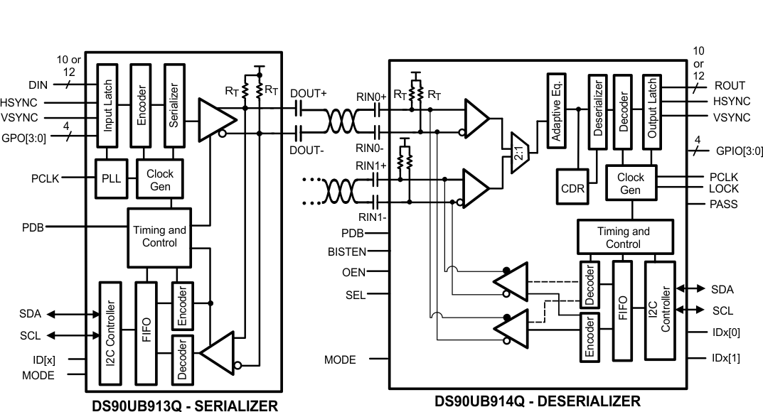
The DS90UB91xQ-Q1 FPD-Link III chipsets are intended to link megapixel camera imagers and video processors in ECUs. The serializer and deserializer chipset can operate from 10-MHz to 100-MHz pixel clock frequency. The DS90UB913Q-Q1 device transforms a 10- and 12-bit wide parallel LVCMOS data bus along with a bidirectional control channel control bus into a single high-speed differential pair. The high-speed serial bit stream contains an embedded clock and DC-balanced information which enhances signal quality to support AC coupling. The DS90UB914Q-Q1 device receives the single serial data stream and converts it back into a 10- and 12-bit wide parallel data bus together with the control channel data bus. The DS90UB91xQ-Q1 chipsets can accept up to:
- 12 bits of DATA+2 bits SYNC for an input PCLK range of 10 MHz-50 MHz in the 12-bit low-frequency mode
- 12 bits DATA + 2 SYNC bits for an input PCLK range of 15 MHz to 75 MHz in the 12-bit high-frequency mode
- 10 bits DATA + 2 SYNC bits for an input PCLK range of 20 MHz to 100 MHz in the 10-bit mode.
The DS90UB914Q-Q1 chipset has a 2:1 multiplexer that allows customers to select between two serializer inputs. The control channel function of the DS90UB91xQ-Q1 chipset provides bidirectional communication between the image sensor and ECUs. The integrated bidirectional control channel transfers data bidirectionally over the same differential pair used for video data interface. This interface offers advantages over other chipsets by eliminating the need for additional wires for programming and control. The bidirectional control channel bus is controlled through an I2C port. The bidirectional control channel offers asymmetrical communication and is not dependent on video blanking intervals.
The DS90UB91xQ-Q1 chipset offer customers the choice to work with different clocking schemes. The DS90UB91xQ-Q1 chipsets can use an external oscillator as the reference clock source for the PLL or PCLK from the imager as primary reference clock to the PLL.
10.2 Functional Block Diagram
10.3 Feature Description
10.3.1 Serial Frame Format
The high-speed forward channel is composed of 28 bits of data containing video data, sync signals, I2C and parity bits. This data payload is optimized for signal transmission over an AC-coupled link. Data is randomized, balanced and scrambled. The 28-bit frame structure changes in the 12-bit low-frequency mode, 12-bit high frequency mode and the 10-bit mode internally and is seamless to the customer. The bidirectional control channel data is transferred over the single serial link along with the high-speed forward data. This architecture provides a full duplex low-speed forward and backward path across the serial link together with a high-speed forward channel without the dependence on the video blanking phase.
10.3.2 Line Rate Calculations for the DS90UB91xQ
The DS90UB913Q-Q1 device divides the clock internally by divide-by-1 in the 12-bit low-frequency mode, by divide-by-2 in the 10-bit mode and by divide-by-1.5 in the 12-bit high-frequency mode. Conversely, the DS90UB914Q-Q1 multiplies the recovered serial clock to generate the proper pixel clock output frequency. Thus the maximum line rate in the three different modes remains 1.4 Gbps. The following are the formulae used to calculate the maximum line rate in the different modes.
- For 12-bit low-frequency mode, Line rate = fPCLK × 28; that is, fPCLK= 50 MHz, line rate = 50 × 28 = 1.4 Gbps
- For 10-bit mode, Line rate = fPCLK / 2 × 28; that is, fPCLK= 100 MHz, line rate = (100 / 2) × 28 = 1.4 Gbps
- For the 12-bit high-frequency mode, Line rate = fPCLK × (2 / 3) × 28; that is, fPCLK= 75 MHz, line rate = (75) × (2 / 3) × 28 = 1.4 Gbps
10.3.3 Deserializer Multiplexer Input
The DS90UB914Q-Q1 offers a 2:1 multiplexer that can be used to select which camera is used as the input. Figure 25 shows the operation of the 2:1 multiplexer in the deserializer. The selection of the camera can be pin controlled as well as register controlled. Both the deserializer inputs cannot be enabled at the same time. If the Serializer A is selected as the active serializer, the back-channel for Deserializer A turns ON and vice versa. To switch between the two cameras, first the Serializer B has to be selected using the SEL pin/register on the deserializer. After that the back channel driver for Deserializer B has to be enabled using the register in the deserializer.
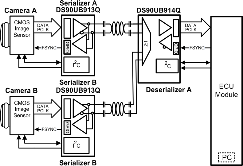 Figure 25. Using the Multiplexer on the Deserializer to Enable a Two-Camera System
10.3.4 Error Detection
The chipset provides error detection operations for validating data integrity in long distance transmission and reception. The data error detection function offers users flexibility and usability of performing bit-by-bit data transmission error checking. The error detection operating modes support data validation of the following signals:
- Bidirectional control channel data across the serial link
- Parallel video/sync data across the serial link
The chipset provides one parity bit on the forward channel and 4 CRC bits on the back channel for error detection purposes. The DS90UB91xQ-Q1 chipset checks the forward and back channel serial links for errors and stores the number of detected errors in two 8-bit registers in the serializer and the deserializer respectively.
To check parity errors on the forward-channel, monitor registers 0x1A and 0x1B on the deserializer. If there is a loss of LOCK, then the counters on registers 0x1A and 0x1B are reset.
NOTE
Whenever there is a parity error on the forward channel, the PASS pin will go low.
To check CRC errors on the back-channel, monitor registers 0x0A and 0x0B on the serializer.
10.3.5 Description of Bidirectional Control Bus and I2C Modes
The I2C-compatible interface allows programming of the DS90UB913Q-Q1, DS90UB914Q-Q1, or an external remote device (such as image sensor) through the bidirectional control channel. Register programming transactions to/from the DS90UB913xQ-Q1 chipset are employed through the clock (SCL) and data (SDA) lines. These two signals have open-drain I/Os and both lines must be pulled up to VDDIO by an external resistor. Pullup resistors or current sources are required on the SCL and SDA busses to pull them high when they are not being driven low. A logic LOW is transmitted by driving the output low. Logic HIGH is transmitted by releasing the output and allowing it to be pulled up externally. The appropriate pullup resistor values will depend upon the total bus capacitance and operating speed. The DS90UB91xQ-Q1 I2C bus data rate supports up to 400 kbps according to I2C fast mode specifications.
 Figure 26. Write Byte
 Figure 27. Read Byte
 Figure 28. Basic Operation
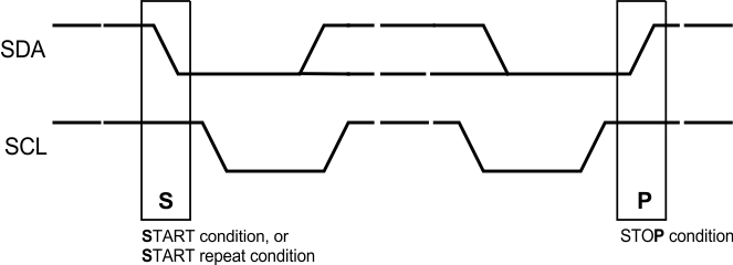 Figure 29. Start and Stop Conditions
10.3.6 Slave Clock Stretching
The I2C-compatible interface allows programming of the DS90UB913Q-Q1, DS90UB914Q-Q1, or an external remote device (such as image sensor) through the bidirectional control.
NOTE
To communicate and synchronize with remote devices on the I2C bus through the bidirectional control channel/MCU, the chipset utilizes bus clock stretching (holding the SCL line low) during data transmission where the I2C slave pulls the SCL line low on the 9th clock of every I2C transfer (before the ACK signal).
The slave device will not control the clock and only stretches it until the remote peripheral has responded. The I2C master must support clock stretching to operate with the DS90UB91xQ-Q1 chipset.
10.3.7 I2C Pass-Through
I2C pass-through provides an alternative means to independently address slave devices. The mode enables or disables I2C bidirectional control channel communication to the remote I2C bus. This option is used to determine whether or not an I2C instruction is to be transferred over to the remote I2C device. When enabled, the I2C bus traffic will continue to pass through, I2C commands will be excluded to the remote I2C device. The pass-through function also provides access and communication to only specific devices on the remote bus.
See Figure 30 for an example of this function.
If master controller transmits I2C transaction for address 0xA0, the SER A with I2C pass-through enabled will transfer I2C commands to remote Camera A. The SER B with I2C pass-through disabled, any I2C commands will be bypassed on the I2C bus to Camera B.
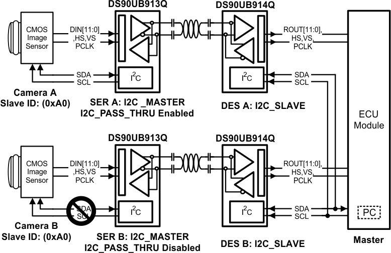 Figure 30. I2C Pass-Through
10.3.8 ID[x] Address Decoder on the Serializer
The ID[x] pin on the serializer is used to decode and set the physical slave address of the serializer (I2C only) to allow up to five devices on the bus connected to the serializer using only a single pin. The pin sets one of the 5 possible addresses for each serializer device. The pin must be pulled to VDD (1.8 V, not VDDIO) with a 10-kΩ resistor and a pulldown resistor (RID) of the recommended value to set the physical device address. The recommended maximum resistor tolerance is 1%.
![DS90UB913Q-Q1 DS90UB914Q-Q1 ID[x] Address Decoder on the
Serializer DS90UB913Q-Q1 DS90UB914Q-Q1 30144673.gif](/ods/images/ZHCSDZ6D/30144673.gif) Figure 31. ID[x] Address Decoder on the Serializer
Figure 31. ID[x] Address Decoder on the Serializer
Table 1. ID[x] Resistor Value for DS90UB913Q-Q1 Serializer
| ID[x] Resistor Value — DS90UB913Q-Q1 Serializer | ||
|---|---|---|
| Resistor RID0 Ω
(1% Tolerance) |
Address 7'b | Address 8'b 0 appended (WRITE) |
| 0 k | 0x58 | 0xB0 |
| 2 k | 0x59 | 0xB2 |
| 4.7 k | 0x5A | 0xB4 |
| 8.2 k | 0x5B | 0xB6 |
| 14 k | 0x5C | 0xB8 |
| 100 k | 0x5D | 0xBA |
10.3.9 ID[x] Address Decoder on the Deserializer
The IDx[0] and IDx[1] pins on the deserializer are used to decode and set the physical slave address of the deserializer (I2C only) to allow up to 16 devices on the bus using only two pins. The pins set one of 16 possible addresses for each deserializer device. As there will be more deserializer devices connected on the same board than serializers, more I2C device addresses have been defined for the DS90UB914Q-Q1 deserializer than the DSDS90UB913Q-Q1 serializer. The pins must be pulled to VDD (1.8 V, not VDDIO) with a 10-kΩ resistor and two pulldown resistors (RID0 and RID1) of the recommended value to set the physical device address. The recommended maximum resistor tolerance is 1%.
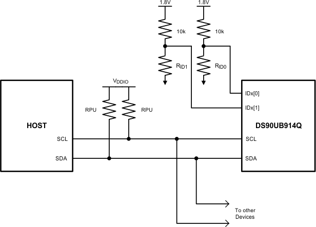 Figure 32. ID[x[ Address Decoder on the Deserializer
Table 2. Resistor Values for IDx[0] and IDx[1] on DS90UB914Q-Q1 Deserializer
| ID[X] RESISTOR VALUE — DS90UB913Q SERIALIZER | |||
|---|---|---|---|
| RESISTOR RID1 Ω
(1%TOLERANCE) |
RESISTOR RID0 Ω
(1%TOLERANCE) |
ADDRESS 7'b | ADDRESS 8'b 0 APPENDED (WRITE) |
| 0 k | 0 k | 0x60 | 0xC0 |
| 0 k | 3 k | 0x61 | 0xC2 |
| 0 k | 11 k | 0x62 | 0xC4 |
| 0 k | 100 k | 0x63 | 0xC6 |
| 3 k | 0 k | 0x64 | 0xC8 |
| 3 k | 3 k | 0x65 | 0xCA |
| 3 k | 11 k | 0x66 | 0XCC |
| 3 k | 100 k | 0x67 | 0XCE |
| 11 k | 0 k | 0x68 | 0XD0 |
| 11 k | 3 k | 0x69 | 0XD2 |
| 11 k | 11 k | 0x6A | 0XD4 |
| 11 k | 100 k | 0x6B | 0XD6 |
| 100 k | 0 k | 0x6C | 0XD8 |
| 100 k | 3 k | 0x6D | 0XDA |
| 100 k | 11 k | 0x6E | 0XDC |
| 100 k | 100 k | 0x6F | 0XDE |
10.3.10 Programmable Controller
An integrated I2C slave controller is embedded in the DS90UB913Q-Q1 serializer as well as the DS90UB914Q-Q1 deserializer. It must be used to configure the extra features embedded within the programmable registers or it can be used to control the set of programmable GPIOs.
10.3.11 Synchronizing Multiple Cameras
For applications requiring multiple cameras for frame-synchronization, TI recommends to utilize the General-Purpose Input/Output (GPIO) pins to transmit control signals to synchronize multiple cameras together. To synchronize the cameras properly, the system controller needs to provide a field sync output (such as a vertical or frame sync signal) and the cameras must be set to accept an auxiliary sync input. The vertical synchronize signal corresponds to the start and end of a frame and the start and end of a field.
NOTE
this form of synchronization timing relationship has a non-deterministic latency. After the control data is reconstructed from the bidirectional control channel, there will be a time variation of the GPIO signals arriving at the different target devices (between the parallel links). The maximum latency delta (t1) of the GPIO data transmitted across multiple links is 25 µs.
NOTE
The user must verify that the timing variations between the different links are within their system and timing specifications.
See Figure 33 for an example of synchronizing multiple cameras.
The maximum time (t1) between the rising edge of GPIO (that is, sync signal) arriving at Camera A and Camera B is 25 µs.
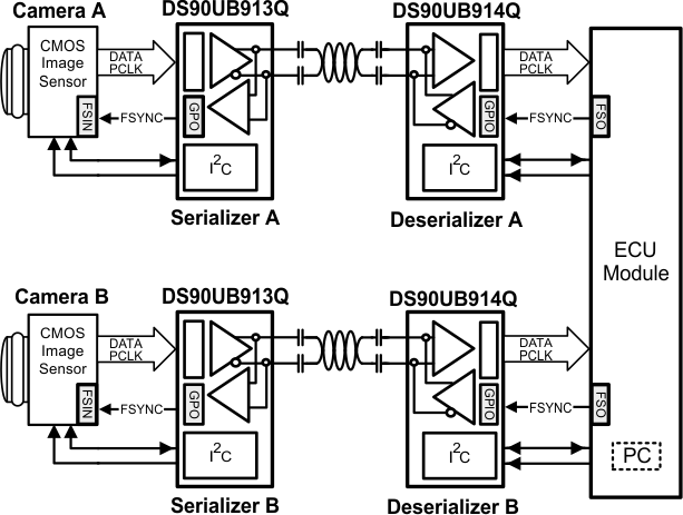 Figure 33. Synchronizing Multiple Cameras
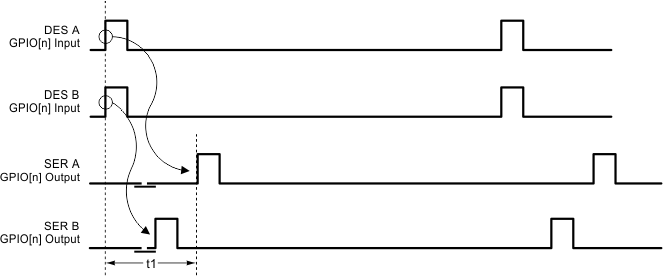 Figure 34. GPIO Delta Latency
10.3.12 General-Purpose I/O (GPIO) Descriptions
There are 4 GPOs on the serializer and 4 GPIOs on the deserializer when the DS90UB91xQ-Q1 chipsets are run off the pixel clock from the imager as the reference clock source. The GPOs on the serializer can be configured as outputs for the input signals that are fed into the deserializer GPIOs. In addition, the GPOs on the serializer can behave as outputs of the local register on the serializer. The GPIOs on the deserializer can be configured to be the input signals feeding the output of the GPOs on the serializer. In addition the GPIOs on the deserializer can be configured to behave as outputs of the local register on the deserializer. If the DS90UB91xQ-Q1 chipsets are run off the external oscillator source as the reference clock, then GPO3 on the serializer is automatically configured to be the input for the external clock and GPIO2 on the deserializer is configured to be the output of the divide-by-2 clock which is fed into the imager as its reference clock. In this case, the GPIO2 and GPIO3 on the deserializer can only behave as outputs of the local register on the deserializer. The GPIO maximum switching rate is up to 66 kHz when configured for communication between deserializer GPIO to serializer GPO.
10.3.13 LVCMOS VDDIO Option
1.8-V, 2.8-V, and 3.3-V serializer inputs and 1.8-V and 3.3-V deserializer outputs are user configurable to provide compatibility with 1.8-V, 2.8-V and 3.3-V system interfaces.
10.3.14 Deserializer – Adaptive Input Equalization (AEQ)
The receiver inputs provide an adaptive input equalization filter in order to compensate for loss from the media. The level of equalization can also be manually selected through register controls. The fully-adaptive equalizer output can be seen using the CMLOUTP/CMLOUTN pins in the deserializer.
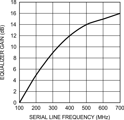 Figure 35. Maximum Equalizer Gain vs. Line Frequency
10.3.15 EMI Reduction
10.3.15.1 Deserializer Staggered Output
The receiver staggers output switching to provide a random distribution of transitions within a defined window. Outputs transitions are distributed randomly. This minimizes the number of outputs switching simultaneously and helps to reduce supply noise. In addition it spreads the noise spectrum out reducing overall EMI.
10.3.15.2 Spread Spectrum Clock Generation (SSCG) on the Deserializer
The DS90UB914Q-Q1 parallel data and clock outputs have programmable SSCG ranges from 10 MHz to 100 MHz. The modulation rate and modulation frequency variation of output spread is controlled through the SSC control registers on the DS90UB914Q-Q1 device. SSC profiles can be generated using bits [3:0] in register 0x02 in the deserializer.
10.4 Device Functional Modes
10.4.1 DS90UB91xQ-Q1 Operation With External Oscillator as Reference Clock
In some applications, the pixel clock that comes from the imager can have jitter which exceeds the tolerance of the DS90UB91xQ-Q1 chipsets. In this case, the DS90UB913Q-Q1 device should be operated by using an external clock source as the reference clock for the DS90UB91xQ-Q1 chipsets. This is the recommended operating mode. The external oscillator clock output goes through a divide-by-2 circuit in the DS90UB913Q-Q1 serializer and this divided clock output is used as the reference clock for the imager. The output data and pixel clock from the imager are then fed into the DS90UB913Q-Q1 device. Figure 36 shows the operation of the DS90UB1xQ-Q1 chipsets while using an external automotive grade oscillator.
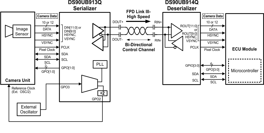 Figure 36. DS90UB91xQ-Q1 Operation in the External Oscillator Mode
When the DS90UB913Q-Q1 device is operated using an external oscillator, the GPO3 pin on the
DS90UB913Q-Q1 is the input pin for the external oscillator. In applications where the DS90UB913Q-Q1 device is operated from an external oscillator, the divide-by-2 circuit in the DS90UB913Q-Q1 device feeds back the divided clock output to the imager device through GPO2 pin. The pixel clock to external oscillator ratios needs to be fixed for the 12-bit high-frequency mode and the 10-bit mode.
NOTE
In the 10-bit mode, the pixel clock frequency divided by the external oscillator frequency must be 2. In the 12-bit high-frequency mode, the pixel clock frequency divided by the external oscillator frequency must be 1.5.
For example, if the external oscillator frequency is 48 MHz in the 10-bit mode, the pixel clock frequency of the imager needs to be twice of the external oscillator frequency, that is, 96 MHz. If the external oscillator frequency is 48 MHz in the 12-bit high-frequency mode, the pixel clock frequency of the imager needs to be 1.5 times of the external oscillator frequency, that is, 72 MHz. In this mode, GPO2 and GPO3 on the serializer cannot act as the output of the input signal coming from GPIO2 or GPIO3 on the deserializer.
10.4.2 DS90UB91xQ-Q1 Operation With Pixel Clock from Imager as Reference Clock
The DS90UB91xQ-Q1 chipsets can be operated by using the pixel clock from the imager as the reference clock.Figure 37 shows the operation of the DS90UB91xQ-Q1 chipsets using the pixel clock from the imager. If the DS90UB913Q-Q1 device is operated using the pixel clock from the imager as the reference clock, then the imager uses an external oscillator as its reference clock. There are 4 GPIOs on the serializer and 4 GPIOs on the deserializer in this mode.
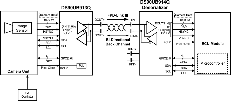 Figure 37. DS90UB91xQ-Q1 Operation in PCLK mode
10.4.3 MODE Pin on Serializer
The mode pin on the serializer can be configured to select if the DS90UB913Q-Q1 device is to be operated from the external oscillator or the PCLK from the imager. The pin must be pulled to VDD (1.8 V, not VDDIO) with a
10-kΩ resistor and a pulldown resistor (RMODE) of the recommended value to set the modes shown in Figure 38. The recommended maximum resistor tolerance is 1%.
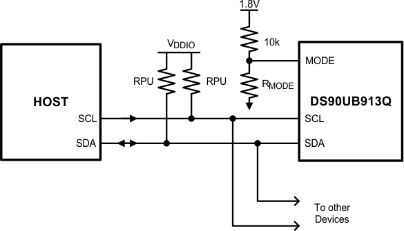 Figure 38. MODE Pin Configuration on DS90UB913Q-Q1
10.4.4 MODE Pin on Deserializer
The mode pin on the deserializer can be used to configure the device to work in the 12-bit low-frequency mode, 12-bit high frequency mode or the 10-bit mode of operation. Internally, the DS90UB91xQ-Q1 chipset operates in a divide-by-1 mode in the 12-bit low-frequency mode, divide-by-2 mode in the 10-bit mode and a divide-by-1.5 mode in the 12-bit high-frequency mode. The pin must be pulled to VDD (1.8 V, not VDDIO) with a 10-kΩ resistor and a pulldown resistor (RMODE) of the recommended value to set the different modes in the deserializer as mentioned in Table 4. The deserializer automatically configures the serializer to correct mode through the back-channel. The recommended maximum resistor tolerance is 1%
.
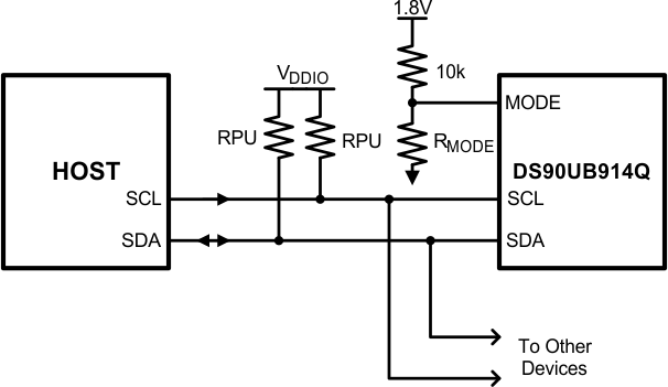 Figure 39. Mode Pin Configuration on DS90UB914Q-Q1 Deserializer
Table 4. DS90UB914Q-Q1 Deserializer MODE Resistor Value
| DS90UB914Q-Q1 DESERIALIZER MODE RESISTOR VALUE | |
|---|---|
| MODE SELECT | RMODE RESISTOR VALUE |
| 12-bit low-frequency mode 10 to 50 MHz PCLK 10 to 12 bit DATA + 2 SYNC |
0 Ω |
| 12-bit low-frequency mode 15 to 75 MHz PCLK 10 to 12 bit DATA + 2 SYNC |
3 kΩ |
| 10-bit mode 20 to 100 MHz PCLK 10 to 10 bit DATA + 2 SYNC |
11 kΩ |
10.4.5 Clock-Data Recovery Status Flag (LOCK), Output Enable (OEN) and Output State Select (OSS_SEL)
When PDB is driven HIGH, the CDR PLL of the deserializer begins locking to the serial input and LOCK is TRI-STATE or LOW (depending on the value of the OEN setting). After the DS90UB914Q-Q1 completes its lock sequence to the input serial data, the LOCK output is driven HIGH, indicating valid data and clock recovered from the serial input is available on the parallel bus and PCLK outputs. The states of the outputs are based on the OEN and OSS_SEL setting (Table 3). See Figure 20.
Table 5. Output States
| INPUTS | OUTPUTS | ||||||
|---|---|---|---|---|---|---|---|
| SERIAI INPUTS | PDB | OEN | OSS | LOCK | PASS | DATA, GPIO, I2S | CLK |
| X | 0 | X | X | Z | Z | Z | Z |
| X | 1 | 0 | 0 | L or H | L | L | L |
| X | 1 | 0 | 1 | L or H | Z | Z | Z |
| Static | 1 | 1 | 0 | L | L | L | L/Osc (Register Bit Enable) |
| Static | 1 | 1 | 1 | H | Previous State | L | L |
| Active | 1 | 1 | 0 | H | L | L | L |
| Active | 1 | 1 | 1 | H | Valid | Valid | Valid |
10.4.6 Multiple Device Addressing
Some applications require multiple camera devices with the same fixed address to be accessed on the same I2C bus. The DS90UB91xQ-Q1 provides slave ID matching/aliasing to generate different target slave addresses when connecting more than two identical devices together on the same bus. This allows the slave devices to be independently addressed. Each device connected to the bus is addressable through a unique ID by programming of the SLAVE_ID_MATCH register on deserializer. This will remap the SLAVE_ID_MATCH address to the target SLAVE_ID_INDEX address; up to 8 ID indexes are supported. The ECU Controller must keep track of the list of I2C peripherals in order to properly address the target device.
See Figure 40 for an example of multiple device addressing.
- ECU is the I2C master and has an I2C master interface
- The I2C interfaces in DES A and DES B are both slave interfaces
- The I2C protocol is bridged from DES A to SER A and from DES B to SER B
- The I2C interfaces in SER A and SER B are both master interfaces
If master controller transmits I2C slave 0xA0, the DES A address 0xC0 will forward the transaction to remote Camera A. If the controller transmits slave address 0xA4, the DES B 0xC2 will recognize that 0xA4 is mapped to 0xA0 and will be transmitted to the remote Camera B. If controller sends command to address 0xA6, the DES B 0xC2 will forward transaction to slave device 0xA2.
The Slave ID index/match is supported only in the camera mode (SER: MODE pin = L; DES: MODE pin = H). For Multiple device addressing in display mode (SER: MODE pin = H; DES: MODE pin = L), use the I2C pass-through function.
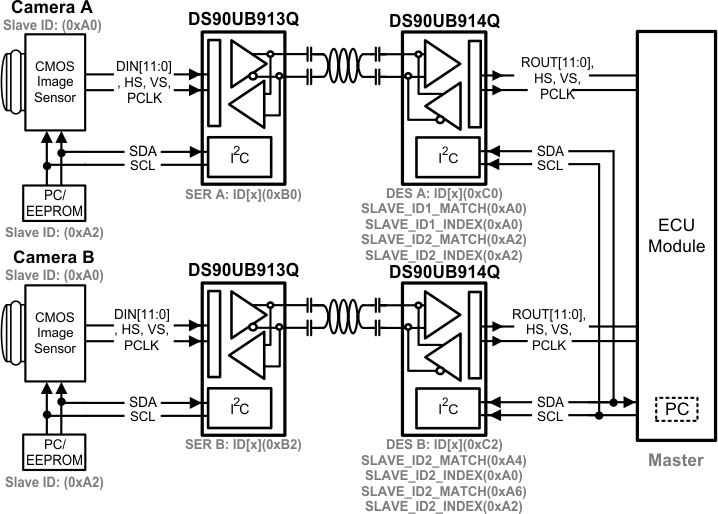 Figure 40. Multiple Device Addressing
10.4.7 Powerdown
The SER has a PDB input pin to ENABLE or Powerdown (SLEEP) the device. The modes can be controlled by the host and is used to disable the Link to save power when the remote device is not operational. In this mode, if the PDB pin is tied High and the SER will enter SLEEP when the PCLK stops. When the PCLK starts again, the SER will then lock to the valid input PCLK and transmit the data to the DES. In SLEEP mode, the high-speed driver outputs are static (High). The DES has a PDB input pin to ENABLE or Powerdown (SLEEP) the device. This pin can be controlled by the system and is used to disable the DES to save power. An auto mode is also available. In this mode, the PDB pin is tied High and the DES will enter SLEEP when the serial stream stops. When the serial stream starts up again, the DES will lock to the input stream and assert the LOCK pin and output valid data. In SLEEP mode, the Data and PCLK outputs are set by the OSS_SEL configuration.
10.4.8 Pixel Clock Edge Select (TRFB / RRFB)
The TRFB/RRFB selects which edge of the Pixel Clock is used. For the SER, this register determines the edge that the data is latched on. If TRFB register is 1, data is latched on the Rising edge of the PCLK. If TRFB register is 0, data is latched on the Falling edge of the PCLK. For the DES, this register determines the edge that the data is strobed on. If RRFB register is 1, data is strobed on the Rising edge of the PCLK. If RRFB register is 0, data is strobed on the falling edge of the PCLK.
 Figure 41. Programmable PCLK Strobe Select
10.4.9 Power-Up Requirements and PDB Pin
When power is applied, the VDDIO supply needs to reach the expected operating voltage (1.8 V to 3.3 V) before the other supplies (VDDn) begin to ramp. It is required to delay and release the PDB Signal after VDD (VDDn and VDDIO) power supplies have settled to the recommended operating voltage. An external RC network can be connected to the PDB pin to ensure PDB arrives after all the VDD has stabilized.
 Figure 42. Power-Up Sequencing
10.4.10 Built-In Self Test
An optional AT-Speed, Built-In Self Test (BIST) feature supports the testing of the high-speed serial link and low-speed back channel. This is useful in the prototype stage, equipment production, and in-system test and also for system diagnostics.
10.4.11 BIST Configuration and Status
The chipset can be programmed into BIST mode using either pins or registers. By default BIST configuration is controlled through pins. BIST can be configured through registers using BIST Control register (0x24). Pin based configuration is defined as follows:
- BISTEN : Enable the BIST Process
- GPIO0 and GPIO1 : Defines the BIST clock source (PCLK vs. various frequencies of internal OSC
Table 6. BIST Configuration
| DESERIALIZER GPIO[0:1] | OSCILLATOR SOURCE | BIST FREQUENCY (MHZ) |
|---|---|---|
| 00 | External PCLK | PCLK or External Oscillator |
| 01 | Internal | 50 |
| 10 | Internal | 25 |
| 11 | Internal | 12.5 |
The BIST mode provides various options for source PCLK. Using external pins, GPIO0 and GPIO1 or using registers, customer can program the BIST mode to use external PCLK or various OSC frequencies. The BIST status can be monitored real time on PASS pin. For every frame with error(s), PASS pin toggles low for half PCLK period. If two consecutive frames have errors, PCLK will toggle twice to allow counting of frames with errors. Once the BIST is done, the PASS pin reflects the pass/fail status of the last BIST run. The status can also be read through I2C for the number of frames in errors. BIST status on PASS pin remains until it is changed by a new BIST session or a reset. The BIST status on PASS pin is not maintained till RX loses LOCK after BISTEN is deassserted. To evaluate BIST in the external oscillator mode, both external oscillator and PCLK need to be present.
The BIST status on PASS pin is not maintained till RX loses LOCK after BISTEN is deassserted. So for all practical purposes, the BIST status can be monitored from register 0x25, that is, BIST Error Count on the DS90UB914Q-Q1 deserializer. To evaluate BIST in the external oscillator mode, both external oscillator and PCLK need to be present.
10.4.11.1 Sample BIST Sequence
Step 1. For the DS90UB91xQ-Q1 FPD-Link III chipset, BIST Mode is enabled through the BISTEN pin of DS90UB914Q-Q1 FPD-Link III deserializer. The desired clock source is selected through the GPIO0 and GPIO1 pins as shown in Table 4.
Step 2. The DS90UB913Q-Q1 serializer is woken up through the back channel if it is not already on. The SSO pattern on the data pins is send through the FPD-Link III to the deserializer. Once the serializer and deserializer are in the BIST mode and the deserializer acquires Lock, the PASS pin of the deserializer goes high and BIST starts checking data stream. If an error in the payload is detected the PASS pin will switch low for one half of the clock period. During the BIST test, the PASS output can be monitored and counted to determine the payload error rate.
Step 3. To stop the BIST mode, the deserializer BISTEN pin is set low. The deserializer stops checking the data. The final test result is not maintained on the PASS pin. To monitor the BIST status, check the BIST Error Count register, 0x25 on the deserializer.
Step 4. The link returns to normal operation after the deserailzer BISTEN pin is low. Figure 44 shows the waveform diagram of a typical BIST test for two cases. Case 1 is error free, and Case 2 shows one with multiple errors. In most cases, it is difficult to generate errors due to the robustness of the link (differential data transmission, and so forth), thus they may be introduced by greatly extending the cable length, faulting the interconnect, or by reducing signal condition enhancements (RX equalization).
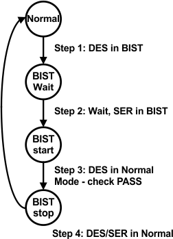 Figure 43. AT-Speed BIST System Flow Diagram
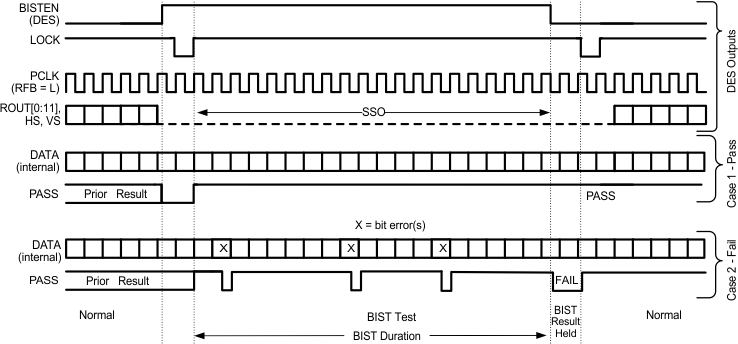 Figure 44. BIST Timing Diagram
10.5 Register Maps
Table 7. DS90UB913Q-Q1 Control Registers
| ADDR (HEX) | NAME | BITS | FIELD | R/W | DEFAULT | DESCRIPTION |
|---|---|---|---|---|---|---|
| 0x00 | I2C Device ID | 7:1 | DEVICE ID | RW | 0x58'h | 7-bit address of serializer; 0x58'h (0101_1000X'b) default |
| 0 | SER ID SEL | 0: Device ID is from ID[x] 1: Register I2C Device ID overrides ID[x] |
||||
| 0x01 | Power and Reset | 7 | RSVD | Reserved | ||
| 6 | RDS | RW | 0 | Digital Output Drive Strength 1: High Drive Strength 0: Low Drive Strength |
||
| 5 | VDDIO Control | RW | 1 | Auto Voltage Control 1: Enable 0: Disable |
||
| 4 | VDDIO MODE | RW | 1 | VDDIOVoltage set 0: 1.8V 1: 3.3V |
||
| 3 | ANAPWDN | RW | 0 | This register can be set only through local I2C access 1: Analog power-down : Powers Down the analog block in the serializer 0: No effect |
||
| 2 | RSVD | RW | 0 | Reserved | ||
| 1 | DIGITAL RESET1 |
RW | 0 | 1: Resets the digital block except for register values values. Does not affect device I2C Bus or Device ID. This bit is self-clearing. 0: Normal Operation |
||
| 0 | DIGITAL RESET0 | RW | 1 | 1: Digital Reset, resets the entire digital block including all register values.This bit is self-clearing. 0: Normal Operation. |
||
| 0x02 | RESERVED | |||||
| 0x03 | General Configuration | 7 | RX CRC Checker Enable | RW | 1 | Back-channel CRC Checker Enable 1:Enabled 0:Disabled |
| 6 | TX Parity Generator Enable | RW | 1 | Forward channel Parity Generator Enable 1: Enable 0: Disable |
||
| 5 | CRC Error Reset | RW | 0 | Clear CRC Error Counters. This bit is NOT self-clearing. 1: Clear Counters 0: Normal Operation |
||
| 4 | I2C Remote Write Auto Acknowledge | RW | 0 | Automatically Acknowledge I2C Remote Write The mode works when the system is LOCKed. 1: Enable: When enabled, I2C writes to the deserializer (or any remote I2C Slave, if I2C PASS ALL is enabled) are immediately acknowledged without waiting for the deserializer to acknowledge the write. The accesses are then re-mapped to address specified in 0x06. 0: Disable |
||
| 3 | I2C Pass All | RW | 0 | 1: Enable Forward Control Channel pass-through of all I2C accesses to I2C Slave IDs that do not match the Serializer I2C Slave ID. The I2C accesses are then remapped to address specified in register 0x06.
0: Enable Forward Control Channel pass-through only of I2C accesses to I2C Slave IDs matching either the remote Deserializer Slave ID or the remote Slave ID. |
||
| 2 | I2C PASSTHROUGH | RW | 1 | I2C Pass-Through Mode 0: Pass-Through Disabled 1: Pass-Through Enabled |
||
| 0x03 | General Configuration | 1 | OV_CLK2PLL | RW | 0 | 1:Enabled : When enabled this registers overrides the clock to PLL mode (External Oscillator mode or Direct PCLK mode) defined through MODE pin and allows selection through register 0x35 in the serializer 0: Disabled : When disabled, Clock to PLL mode (External Oscillator mode or Direct PCLK mode) is defined through MODE pin on the serializer. |
| 0 | TRFB | RW | 1 | Pixel Clock Edge Select 1: Parallel Interface Data is strobed on the Rising Clock Edge. 0: Parallel Interface Data is strobed on the Falling Clock Edge. |
||
| 0x04 | RESERVED | |||||
| 0x05 | Mode Select | 7 | RSVD | RW | 0 | Reserved |
| 6 | RSVD | RW | 0 | Reserved. | ||
| 5 | MODE_OVERRIDE | RW | 0 | Allows overriding mode select bits coming from back-channel 1: Overrides MODE select bits 0: Does not override MODE select bits |
||
| 4 | MODE_UP To DATE | R | 0 | Indicates that the status of mode select from deserializer is up to date | ||
| 3 | Pin_MODE_12–bit High Frequency | R | 0 | 1: 12-bit high-frequency mode is selected. 0: 12-bit high-frequency mode is not selected. |
||
| 2 | Pin_MODE_10–bit mode | R | 0 | 1: 10-bit mode is selected. 0: 10-bit mode is not selected. |
||
| 1:0 | RSVD | Reserved | ||||
| 0x06 | DES ID | 7:1 | Desializer Device ID | RW | 0x00 | 7-bit Deserializer Device ID configures the I2C Slave ID of the remote deserializer. A value of 0 in this field disables I2C access to the remote deserializer. This field is automatically configured by the Bidirectional Control Channel once RX Lock has been detected. Software may overwrite this value, but should also assert the FREEZE DEVICE ID bit to prevent overwriting by the Bidirectional Control Channel. |
| 0 | Freeze Device ID | RW | 0 | 1: Prevents auto-loading of the Deserializer Device ID by the bidirectional control channel. The ID will be frozen at the value written. 0: Update |
||
| 0x07 | DESAlias | 7:1 | Deserializer ALIAS ID | RW | 0 | 7-bit Remote Deserializer Device Alias ID Configures the decoder for detecting transactions designated for an I2C deserializer device. The transaction will be remapped to the address specified in the DES ID register. A value of 0 in this field disables access to the remote I2C Slave. |
| 0 | RSVD | Reserved | ||||
| 0x08 | SlaveID | 7:1 | SLAVE ID | RW | 0x00 | 7-bit Remote Slave Device ID Configures the physical I2C address of the remote I2C Slave device attached to the remote deserializer. If an I2C transaction is addressed to the Slave Alias ID, the transaction will be remapped to this address before passing the transaction across the Bidirectional Control Channel to the deserializer. A value of 0 in this field disables access to the remote I2C slave. |
| 0 | RSVD | Reserved | ||||
| 0x09 | SlaveAlias | 7:1 | SLAVE ALIAS ID | RW | 0x00 | 7-bit Remote Slave Device Alias ID Configures the decoder for detecting transactions designated for an I2C Slave device attached to the remote deserializer. The transaction will be remapped to the address specified in the Slave ID register. A value of 0 in this field disables access to the remote I2C Slave. |
| 0 | RSVD | Reserved | ||||
| 0x0A | CRC Errors | 7:0 | CRC Error Byte 0 | R | 0 | Number of back-channel CRC errors during normal operation. Least Significant byte |
| 0x0B | CRC Errors | 7:0 | CRC Error Byte 1 | R | 0 | Number of back-channel CRC errors during normal operation. Most Significant byte |
| 0x0C | General Status | 7:5 | Rev-ID | R | 0 | Revision ID 0x00: Production |
| 4 | RX Lock Detect | R | 0 | 1: RX LOCKED 0: RX not LOCKED |
||
| 3 | BIST CRC Error Status | R | 0 | 1: CRC errors in BIST mode 0: No CRC errors in BIST mode |
||
| 2 | PCLK Detect | R | 0 | 1: Valid PCLK detected 0: Valid PCLK not detected |
||
| 1 | DES Error | R | 0 | 1: CRC error is detected during communication with deserializer. This bit is cleared upon loss of link or assertion of CRC ERROR RESET in register 0x04. 0: No effect |
||
| 0 | LINK Detect | R | 0 | 1: Cable link detected 0: Cable link not detected This includes any of the following faults — Cable Open — + and - shorted — Short to GND — Short to battery |
||
| 0x0D | GPO[0] and GPO[1] Configuration |
7 | GPO1 Output Value | RW | 0 | Local GPIO Output Value This value is output on the GPIO pin when the GPIO function is enabled, the local GPIO direction is Output, and remote GPIO control is disabled. |
| 6 | GPO1 Remote Enable | RW | 1 | Remote GPIO Control 1: Enable GPIO control from remote deserializer. The GPIO pin needs to be an output, and the value is received from the remote deserializer. 0: Disable GPIO control from remote deserializer. |
||
| 5 | GPO1 Direction | RW | 0 | 1: Input 0: Output |
||
| 4 | GPO0 Enable | RW | 1 | 1: GPIO enable 0: Tri-state |
||
| 3 | GPO0 Output Value | RW | 0 | Local GPIO Output Value This value is output on the GPIO pin when the GPIO function is enabled, the local GPIO direction is Output, and remote GPIO control is disabled. | ||
| 2 | GPO0 Remote Enable | RW | 1 | Remote GPIO Control 1: Enable GPIO control from remote deserializer. The GPIO pin needs to be an output, and the value is received from the remote deserializer. 0: Disable GPIO control from remote deserializer. |
||
| 1 | GPO0 Direction | RW | 0 | 1: Input 0: Output |
||
| 0 | GPO0 Enable | RW | 1 | 1: GPIO enable 0: Tri-state |
||
| 0x0E | GPO[2] and GPO[3] Configuration |
7 | GPO3 Output Value | RW | 0 | Local GPIO Output Value This value is output on the GPIO pin when the GPIO function is enabled, the local GPIO direction is Output, and remote GPIO control is disabled. |
| 6 | GPO3 Remote Enable | RW | 0 | Remote GPIO Control 1: Enable GPIO control from remote deserializer. The GPIO pin needs to be an output, and the value is received from the remote deserializer. 0: Disable GPIO control from remote deserializer. |
||
| 5 | GPO3 Direction | RW | 1 | 1: Input 0: Output |
||
| 4 | GPO3 Enable | RW | 1 | 1: GPIO enable 0: Tri-state |
||
| 3 | GPO2 Output Value | RW | 0 | Local GPIO Output Value This value is output on the GPIO pin when the GPIO function is enabled, the local GPIO direction is Output, and remote GPIO control is disabled. | ||
| 2 | GPO2 Remote Enable | RW | 1 | Remote GPIO Control 1: Enable GPIO control from remote deserializer. The GPIO pin needs to be an output, and the value is received from the remote deserializer. 0: Disable GPIO control from remote deserializer. |
||
| 1 | GPO2 Direction | RW | 0 | 1: Input 0: Output |
||
| 0 | GPO2 Enable | RW | 1 | 1: GPIO enable 0: Tri-state |
||
| 0x0F | I2C Master Config | 7:5 | RSVD | Reserved | ||
| 4:3 | SDA Output Delay | RW | 00 | SDA Output Delay This field configures output delay on the SDA output. Setting this value will increase output delay in units of 50 ns. Nominal output delay values for SCL to SDA are: 00 : 350 ns 01: 400 ns 10: 450 ns 11: 500 ns |
||
| 2 | Local Write Disable | RW | 0 | Disable Remote Writes to Local Registers Setting this bit to a 1 will prevent remote writes to local device registers from across the control channel. This prevents writes to the serializer registers from an I2C master attached to the deserializer. Setting this bit does not affect remote access to I2C slaves at the serializer. | ||
| 1 | I2C Bus Timer Speed up |
RW | 0 | Speed up I2C Bus Watchdog Timer 1: Watchdog Timer expires after approximately 50 microseconds 0: Watchdog Timer expires after approximately 1 second. |
||
| 0 | I2C Bus Timer Disable | RW | 0 | 1. Disable I2C Bus Watchdog Timer When the I2C Watchdog Timer may be used to detect when the I2C bus is free or hung up following an invalid termination of a transaction. If SDA is high and no signaling occurs for approximately 1 second, the I2C bus will assumed to be free. If SDA is low and no signaling occurs, the device will attempt to clear the bus by driving 9 clocks on SCL 0: No effect |
||
| 0x10 | I2C Control | 7 | RSVD | Reserved | ||
| 6:4 | SDA Hold Time | RW | 0x1 | Internal SDA Hold Time. This field configures the amount of internal hold time provided for the SDA input relative to the SCL input. Units are 50 ns. | ||
| 3:0 | I2C Filter Depth | RW | 0x7 | I2C Glitch Filter Depth This field configures the maximum width of glitch pulses on the SCL and SDA inputs that will be rejected. Units are 10 ns. | ||
| 0x11 | SCL High Time | 7:0 | SCL High Time | RW | 0x82 | I2C Master SCL High Time This field configures the high pulse width of the SCL output when the serializer is the Master on the local I2C bus. Units are 50 ns for the nominal oscillator clock frequency. The default value is set to provide a minimum (4µs + 1µs of rise time for cases where rise time is very fast) SCL high time with the internal oscillator clock running at 26MHz rather than the nominal 20 MHz. |
| 0x12 | SCL LOW Time | 7:0 | SCL Low Time | RW | 0x82 | I2C SCL Low Time This field configures the low pulse width of the SCL output when the serializer is the Master on the local I2C bus. This value is also used as the SDA setup time by the I2C Slave for providing data prior to releasing SCL during accesses over the Bidirectional Control Channel. Units are 50 ns for the nominal oscillator clock frequency. The default value is set to provide a minimum (4.7 µs + 0.3 µs of fall time for cases where fall time is very fast) SCL low time with the internal oscillator clock running at 26 MHz rather than the nominal 20 MHz. |
| 0x13 | General-Purpose Control | 7:0 | GPCR[7:0] | RW | 0 | 1: High 0: Low |
| 0x14 | BIST Control | 7:3 | RSVD | Reserved | ||
| 2:1 | Clock Source | RW | 0x0 | Allows choosing different OSC clock frequencies for forward channel frame. OSC Clock Frequency in Functional Mode when OSC mode is selected or when the selected clock source is not present, for example, missing PCLK/ External Oscillator. See Table 9 for oscillator clock frequencies when PCLK/ External Clock is missing. |
||
| 0 | BIST Enable | RW | 0 | BIST Control: 1: Enable BIST mode 0: Disable BIST mode |
||
| 0x15 - 0x1D |
RESERVED | |||||
| 0x1E | BCC Watchdog Control | 7:1 | BCC Watchdog Timer | RW | 0x7F | The watchdog timer allows termination of a control channel transaction if it fails to complete within a programmed amount of time. This field sets the Bidirectional Control Channel Watchdog Timeout value in units of 2ms. This field should not be set to 0. |
| 0 | BCC Watchdog Timer Disable | RW | 0 | Disable Bidirectional Control Channel Watchdog Timer 1: Disables BCC Watchdog Timer operation 0: Enables BCC Watchdog Timer operation |
||
| 0x1F- 0x29 |
RESERVED | |||||
| 0x2A | CRC Errors | 7:0 | BIST Mode CRC Errors Count | R | 0 | Number of CRC Errors in the back channel when in BIST mode |
| 0x2B - 0x34 |
RESERVED | |||||
| 0x35 | PLL Clock Overwrite | 7:4 | RSVD | Reserved | ||
| 3 | PIN_LOCK to External Oscillator | RW | 0 | Status of mode select pin 1: Indicates External Oscillator mode is selected by mode-resistor 0: External Oscillator mode is not selected by mode-resistor |
||
| 2 | PIN_LOCK to Oscillator | RW | 0 | Status of mode select pin 1: Indicates PCLK mode is selected by mode-resistor 0: PCLK mode not selected by mode-resistor |
||
| 1 | LOCK to External Oscillator | RW | 0 | Affects only when 0x03[1]=1 (OV_CLK2PLL) and 0x35[0]=0. 1: Routes GPO3 directly to PLL 0: Allows PLL to lock to PCLK" |
||
| 0 | RSVD | Reserved | ||||
Table 8. DS90UB914Q-Q1 Control Registers
| ADDR (HEX) | NAME | BITS | FIELD | R/W | DEFAULT | DESCRIPTION |
|---|---|---|---|---|---|---|
| 0x00 | I2C Device ID | 7:1 | DEVICE ID | RW | 0x60'h | 7-bit address of deserializer; 0x60h |
| 0 | Deserializer ID Select | RW | 0 | 0: Deserializer Device ID is set using address coming from CAD 1: Register I2C Device ID overrides ID[x] |
||
| 0x01 | Reset | 7:6 | RSVD | Reserved | ||
| 5 | ANAPWDN | RW | 0 | This register can be set only through local I2C access 1: Analog power-down : Powers down the analog block in the serializer 0: No effect |
||
| 4:2 | RSVD | Reserved | ||||
| 1 | Digital Reset 1 | RW | 0 | Digital Reset Resets the entire digital block except registers. This bit is self-clearing. 1: Reset 0: No effect |
||
| 0 | Digital Reset 0 | RW | 0 | Digital Reset Resets the entire digital block including registers. This bit is self-clearing. 1: Reset 0: No effect |
||
| 0x02 | General Configuration 0 | 7 | RSVD | Reserved | ||
| 6 | RSVD | Reserved | ||||
| 5 | Auto-Clock | RW | 0 | 1: Output PCLK or OSC clock when not LOCKED 0: Only PCLK |
||
| 4 | SSCG LFMODE | RW | 0 | 1: Selects 8x mode for 10-18 MHz frequency range in SSCG 0: SSCG running at 4X mode |
||
| 3:0 | SSCG | RW | 0 | SSCG Select 0000: Normal Operation, SSCG OFF 0001: fmod (kHz) PCLK/2168, fdev ±0.50% 0010: fmod (kHz) PCLK/2168, fdev ±1.00% 0011: fmod (kHz) PCLK/2168, fdev ±1.50% 0100: fmod (kHz) PCLK/2168, fdev ±2.00% 0101: fmod (kHz) PCLK/1300, fdev ±0.50% 0110: fmod (kHz) PCLK/1300, fdev ±1.00% 0111: fmod (kHz) PCLK/1300, fdev ±1.50% 1000: fmod (kHz) PCLK/1300, fdev ±2.00% 1001: fmod (kHz) PCLK/868, fdev ±0.50% 1010: fmod (kHz) PCLK/868, fdev ±1.00% 1011: fmod (kHz) PCLK/868, fdev ±1.50% 1100: fmod (kHz) PCLK/868, fdev ±2.00% 1101: fmod (kHz) PCLK/650, fdev ±0.50% 1110: fmod (kHz) PCLK/650, fdev ±1.00% 1111: fmod (kHz) PCLK/650, fdev ±1.50% Note: This register should be changed only after disabling SSCG. |
||
| 0x03 | General Configuration 1 | 7 | RX Parity Checker Enable | RW | 1 | Forward-Channel Parity Checker Enable 1: Enable 0: Disable |
| 6 | TX CRC Checker Enable | RW | 1 | Back-Channel CRC Generator Enable 1: Enable 0: Disable |
||
| 5 | VDDIO Control | RW | 1 | Auto voltage control 1: Enable (auto-detect mode) 0: Disable |
||
| 4 | VDDIO Mode | RW | 0 | VDDIO voltage set 1: 3.3 V 0: 1.8 V |
||
| 0x03 | General Configuration 1 | 3 | I2C Passthrough | RW | 1 | I2C Pass-Through Mode 1: Pass-Through Enabled 0: Pass-Through Disabled |
| 2 | AUTO ACK | RW | 0 | Automatically Acknowledge I2C Remote Write When enabled, I2C writes to the deserializer (or any remote I2C Slave, if I2C PASS ALL is enabled) are immediately acknowledged without waiting for the deserializer to acknowledge the write. The accesses are then remapped to address specified in 0x06. This allows I2C bus without LOCK. 1: Enable 0: Disable |
||
| 1 | Parity Error Reset | RW | 0 | Parity Error Reset, This bit is self-clearing. 1: Parity Error Reset 0: No effect |
||
| 0 | RRFB | RW | 1 | Pixel Clock Edge Select 1: Parallel Interface Data is strobed on the Rising Clock Edge. 0: Parallel Interface Data is strobed on the Falling Clock Edge. |
||
| 0x04 | EQ Feature Control 1 | 7:0 | EQ level - when AEQ bypass is enabled EQ setting is provided by this register | RW | 0x00 | Equalization gain 0x00 = ~0.0 dB 0x01 = ~4.5 dB 0x03 = ~6.5 dB 0x07 = ~7.5 dB 0x0F = ~8.0 dB 0x1F = ~11.0 dB 0x3F = ~12.5 dB |
| 0x05 | RESERVED | |||||
| 0x06 | SER ID | 7:1 | Remote ID | RW | 0x0C | Remote Serializer ID |
| 0 | Freeze Device ID | RW | 0 | Freeze Serializer Device ID Prevent auto-loading of the serializer Device ID from the Forward Channel. The ID will be frozen at the value written. | ||
| 0x07 | SER Alias | 7:1 | Serializer Alias ID | RW | 0x00 | 7-bit Remote Serializer Device Alias ID Configures the decoder for detecting transactions designated for an I2C deserializer device. The transaction will be remapped to the address specified in the SER ID register. A value of 0 in this field disables access to the remote I2C Slave. |
| 0 | RSVD | Reserved | ||||
| 0x08 | Slave ID[0] | 7:1 | Slave ID0 | RW | 0 | 7-bit Remote Slave Device ID 0 Configures the physical I2C address of the remote I2C Slave device attached to the remote serializer. If an I2C transaction is addressed to the Slave Alias ID0, the transaction will be remapped to this address before passing the transaction across the Bidirectional Control Channel to the serializer. |
| 0 | RSVD | Reserved | ||||
| 0x09 | Slave ID[1] | 7:1 | Slave ID1 | RW | 0 | 7-bit Remote Slave Device ID 1 Configures the physical I2C address of the remote I2C Slave device attached to the remote serializer. If an I2C transaction is addressed to the Slave Alias ID1, the transaction will be remapped to this address before passing the transaction across the Bidirectional Control Channel to the serializer. |
| 0 | RSVD | Reserved | ||||
| 0x0A | Slave ID[2] | 7:1 | Slave ID2 | RW | 0x00 | 7-bit Remote Slave Device ID 2 Configures the physical I2C address of the remote I2C Slave device attached to the remote serializer. If an I2C transaction is addressed to the Slave Alias ID2, the transaction will be remapped to this address before passing the transaction across the Bidirectional Control Channel to the serializer. |
| 0 | RSVD | Reserved | ||||
| 0x0B | Slave ID[3] | 7:1 | Slave ID3 | RW | 0 | 7-bit Remote Slave Device ID 3 Configures the physical I2C address of the remote I2C Slave device attached to the remote serializer. If an I2C transaction is addressed to the Slave Alias ID3, the transaction will be remapped to this address before passing the transaction across the Bidirectional Control Channel to the serializer. |
| 0 | RSVD | Reserved | ||||
| 0x0C | Slave ID[4] | 7:1 | Slave ID4 | RW | 0 | 7-bit Remote Slave Device ID 4 Configures the physical I2C address of the remote I2C Slave device attached to the remote serializer. If an I2C transaction is addressed to the Slave Alias ID4, the transaction will be remapped to this address before passing the transaction across the Bidirectional Control Channel to the serializer. |
| 0 | RSVD | Reserved | ||||
| 0x0D | Slave ID[5] | 7:1 | Slave ID5 | RW | 0x00 | 7-bit Remote Slave Device ID 5 Configures the physical I2C address of the remote I2C Slave device attached to the remote serializer. If an I2C transaction is addressed to the Slave Alias ID5 , the transaction will be remapped to this address before passing the transaction across the Bidirectional Control Channel to the serializer. |
| 0 | RSVD | Reserved | ||||
| 0x0E | Slave ID[6] | 7:1 | Slave ID6 | RW | 0 | 7-bit Remote Slave Device ID 6 Configures the physical I2C address of the remote I2C Slave device attached to the remote serializer. If an I2C transaction is addressed to the Slave Alias ID6, the transaction will be remapped to this address before passing the transaction across the Bidirectional Control Channel to the serializer. |
| 0 | RSVD | Reserved | ||||
| 0x0F | Slave ID[7] | 7:1 | Slave ID7 | RW | 0x00 | 7-bit Remote Slave Device ID 7 Configures the physical I2C address of the remote I2C Slave device attached to the remote serializer. If an I2C transaction is addressed to the Slave Alias ID7, the transaction will be remapped to this address before passing the transaction across the Bidirectional Control Channel to the serializer. |
| 0 | RSVD | Reserved | ||||
| 0x10 | Slave Alias[0] | 7:1 | Slave Alias ID0 | RW | 0x00 | 7-bit Remote Slave Device Alias ID 0 Configures the decoder for detecting transactions designated for an I2C Slave device attached to the remote serializer. The transaction will be remapped to the address specified in the Slave ID0 register. A value of 0 in this field disables access to the remote I2C Slave. |
| 0 | RSVD | Reserved | ||||
| 0x11 | Slave Alias[1] | 7:1 | Slave Alias ID1 | RW | 0x00 | 7-bit Remote Slave Device Alias ID 1 Configures the decoder for detecting transactions designated for an I2C Slave device attached to the remote serializer. The transaction will be remapped to the address specified in the Slave ID1 register. A value of 0 in this field disables access to the remote I2C Slave. |
| 0 | RSVD | Reserved | ||||
| 0x12 | Slave Alias[2] | 7:1 | Slave Alias ID2 | RW | 0x00 | 7-bit Remote Slave Device Alias ID 2 Configures the decoder for detecting transactions designated for an I2C Slave device attached to the remote serializer. The transaction will be remapped to the address specified in the Slave ID2 register. A value of 0 in this field disables access to the remote I2C Slave. |
| 0 | RSVD | Reserved | ||||
| 0x13 | Slave Alias[3] | 7:1 | Slave Alias ID3 | RW | 0x00 | 7-bit Remote Slave Device Alias ID 3 Configures the decoder for detecting transactions designated for an I2C Slave device attached to the remote serializer. The transaction will be remapped to the address specified in the Slave ID3 register. A value of 0 in this field disables access to the remote I2C Slave. |
| 0 | RSVD | Reserved | ||||
| 0x14 | Slave Alias[4] | 7:1 | Slave Alias ID4 | RW | 0x00 | 7-bit Remote Slave Device Alias ID 4 Configures the decoder for detecting transactions designated for an I2C Slave device attached to the remote serializer. The transaction will be remapped to the address specified in the Slave ID4 register. A value of 0 in this field disables access to the remote I2C Slave. |
| 0 | RSVD | Reserved | ||||
| 0x15 | Slave Alias[5] | 7:1 | Slave Alias ID5 | RW | 0x00 | 7-bit Remote Slave Device Alias ID 5 Configures the decoder for detecting transactions designated for an I2C Slave device attached to the remote serializer. The transaction will be remapped to the address specified in the Slave ID5 register. A value of 0 in this field disables access to the remote I2C Slave. |
| 0 | RSVD | Reserved | ||||
| 0x16 | Slave Alias[6] | 7:1 | Slave Alias ID6 | RW | 0x00 | 7-bit Remote Slave Device Alias ID 6 Configures the decoder for detecting transactions designated for an I2C Slave device attached to the remote serializer. The transaction will be remapped to the address specified in the Slave ID6 register. A value of 0 in this field disables access to the remote I2C Slave. |
| 0 | RSVD | Reserved | ||||
| 0x17 | Slave Alias[7] | 7:1 | Slave Alias ID7 | RW | 0x00 | 7-bit Remote Slave Device Alias ID 7 Configures the decoder for detecting transactions designated for an I2C Slave device attached to the remote serializer. The transaction will be remapped to the address specified in the Slave ID7 register. A value of 0 in this field disables access to the remote I2C Slave. |
| 0 | RSVD | Reserved | ||||
| 0x18 | Parity Errors Threshold | 7:0 | Parity Error Threshold Byte 0 | RW | 0 | Parity errors threshold on the Forward channel during normal information. This sets the maximum number of parity errors that can be counted using register 0x1A. Least significant Byte. |
| 0x19 | Parity Errors Threshold | 7:0 | Parity Error Threshold Byte 1 | RW | 0 | Parity errors threshold on the Forward channel during normal operation. This sets the maximum number of parity errors that can be counted using register 0x1B. Most significant Byte |
| 0x1A | Parity Errors | 7:0 | Parity Error Byte 0 | RW | 0 | Number of parity errors in the Forward channel during normal operation. Least significant Byte |
| 0x1B | Parity Errors | 7:0 | Parity Error Byte 1 | RW | 0 | Number of parity errors in the Forward channel during normal operation Most significant Byte |
| 0x1C | General Status | 7:4 | Rev-ID | R | 0 | Revision ID 0x0000: Production |
| 3 | RSVD | Reserved | ||||
| 2 | Parity Error | R | 0 | Parity Error detected 1: Parity Errors detected 0: No Parity Errors |
||
| 1 | Signal Detect | R | 0 | 1: Serial input detected 0: Serial input not detected |
||
| 0 | Lock | R | 0 | Deserializer CDR, PLL's clock to recovered clock frequency 1: Deserializer locked to recovered clock 0: Deserializer not locked |
||
| 0x1D | GPIO[1] and GPIO[0] Config | 7 | GPIO1 Output Vaue | RW | 0 | Local GPIO Output Value This value is the output on the GPIO pin when the GPIO function is enabled, the local GPIO direction is Output. |
| 6 | RSVD | Reserved | ||||
| 5 | GPIO1 Direction | RW | 1 | Local GPIO Direction 1: Input 0: Output |
||
| 4 | GPIO1 Enable | RW | 1 | GPIO Function Enable 1: Enable GPIO operation 0: Enable normal operation |
||
| 3 | GPIO0 Output Value | RW | 0 | Local GPIO Output Value This value is output on the GPIO pin when the GPIO function is enabled, the local GPIO direction is Output. | ||
| 0x1D | GPIO[1] and GPIO[0] Config | 2 | RSVD | Reserved | ||
| 1 | GPIO0 Direction | RW | 1 | Local GPIO Direction 1: Input 0: Output |
||
| 0 | GPIO0 Enable | RW | 1 | GPIO Function Enable 1: Enable GPIO operation 0: Enable normal operation |
||
| 0x1E | GPIO[3] and GPIO[2] Config | 7 | GPIO3 Output Vaue | RW | 0 | Local GPIO Output Value This value is the output on the GPIO pin when the GPIO function is enabled, the local GPIO direction is Output. |
| 6 | RSVD | Reserved | ||||
| 5 | GPIO3 Direction | RW | 1 | Local GPIO Direction 1: Input 0: Output |
||
| 4 | GPIO3 Enable | RW | 1 | GPIO Function Enable 1: Enable GPIO operation 0: Enable normal operation |
||
| 3 | GPIO2 Output Value | RW | 0 | Local GPIO Output Value This value is output on the GPIO pin when the GPIO function is enabled, the local GPIO direction is Output. | ||
| 2 | RSVD | Reserved | ||||
| 1 | GPIO2 Direction | RW | 1 | Local GPIO Direction 1: Input 0: Output |
||
| 0 | GPIO2 Enable | RW | 1 | GPIO Function Enable 1: Enable GPIO operation 0: Enable normal operation |
||
| 0x1F | Mode and OSS Select | 7 | OEN_OSS Override | RW | 0 | Allows overriding OEN and OSS select coming from Pins 1: Overrides OEN/OSS_SEL selected by pins 0: Does NOT override OEN/OSS_SEL select by pins |
| 6 | OEN Select | RW | 0 | OEN configuration from register | ||
| 5 | OSS Select | R | 0 | OSS_SEL configuration from register | ||
| 4 | MODE_OVERRIDE | RW | 0 | Allows overriding mode select bits coming from back-channel 1: Overrides MODE select bits 0: Does not override MODE select bits |
||
| 3 | PIN_MODE_12–bit HF mode | R | 0 | Status of mode select pin | ||
| 2 | PIN_MODE_10-bit mode | R | 0 | Status of mode select pin | ||
| 1 | MODE_12–bit High Frequency | RW | 0 | Selects 12-bit high-frequency mode. This bit is automatically updated by the mode settings from RX unless MODE_OVERRIDE is SET 1: 12-bit high-frequency mode is selected. 0: 12-bit high-frequency mode is not selected. |
||
| 0 | MODE_10–bit mode | RW | 0 | Selects 10-bit mode. This bit is automatically updated by the mode settings from RX unless MODE_OVERRIDE is SET 1: Enables 10-bit mode. 0: Disables 10-bit mode. |
||
| 0x20 | BCC Watchdog Control | 7:1 | BCC Watchdog timer | RW | 0 | The watchdog timer allows termination of a control channel transaction if it fails to complete within a programmed amount of time. This field sets the Bidirectional Control Channel Watchdog Timeout value in units of 2ms. This field should not be set to 0. |
| 0 | BCC Watchdog Timer Disable | RW | 0 | Disable Bidirectional Control Channel Watchdog Timer 1: Disables BCC Watchdog Timer operation 0: Enables BCC Watchdog Timer operation |
||
| 0x21 | I2C Control 1 | 7 | I2C pass-through all | RW | 0 | I2C Pass-Through All Transactions 0: Disabled 1: Enabled |
| 6:4 | I2C SDA Hold | RW | 0 | Internal SDA Hold Time This field configures the amount of internal hold time provided for the SDA input relative to the SCL input. Units are 50ns. | ||
| 3:0 | I2C Filter Depth | RW | 0 | I2C Glitch Filter Depth This field configures the maximum width of glitch pulses on the SCL and SDA inputs that will be rejected. Units are 10ns. | ||
| 0x22 | I2C Control 2 | 7 | Forward Channel Sequence Error | R | 0 | Control Channel Sequence Error Detected This bit indicates a sequence error has been detected in forward control channel. 1: If this bit is set, an error may have occurred in the control channel operation 0: No forward channel errors have been detected on the control channel |
| 6 | Clear Sequence Error | RW | 0 | Clears the Sequence Error Detect bit | ||
| 5 | RSVD | Reserved | ||||
| 4:3 | SDA Output Delay | RW | 0 | SDA Output Delay This field configures output delay on the SDA output. Setting this value will increase output delay in units of 50 ns. Nominal output delay values for SCL to SDA are: 00 : 350ns 01: 400ns 10: 450ns 11: 500ns |
||
| 2 | Local Write Disable | RW | 0 | Disable Remote Writes to local registers Setting this bit to a 1 will prevent remote writes to local device registers from across the control channel. This prevents writes to the deserializer registers from an I2C master attached to the serializer. Setting this bit does not affect remote access to I2C slaves at the deserializer. | ||
| 1 | I2C Bus Timer Speed up |
RW | 0 | Speed up I2C Bus Watchdog Timer 1: Watchdog Timer expires after approximately 50 µs 0: Watchdog Timer expires after approximately 1 s. |
||
| 0 | I2C Bus Timer Disable | RW | 0 | Disable I2C Bus Watchdog Timer When the I2C Watchdog Timer may be used to detect when the I2C bus is free or hung up following an invalid termination of a transaction. If SDA is high and no signaling occurs for approximately 1 second, the I2C bus will assumed to be free. If SDA is low and no signaling occurs, the device will attempt to clear the bus by driving 9 clocks on SCL | ||
| 0x23 | General-Purpose Control | 7:0 | GPCR | RW | 0 | Scratch Register |
| 0x24 | BIST Control | 7:4 | RSVD | Reserved | ||
| 3 | BIST Pin Configuration | RW | 1 | Bist Configured through Pin. 1: Bist configured through pin. 0: Bist configured through register bit "reg_24[0]" |
||
| 2:1 | BIST Clock Source | RW | 00 | BIST Clock Source See Table 10 |
||
| 0 | BIST Enable | RW | 0 | BIST Control 1: Enabled 0: Disabled |
||
| 0x25 | Parity Error Count | 7:0 | BIST Error Count | R | 0 | Number of Forward channel Parity errors in the BIST mode. |
| 0x26 - 0x3B |
RESERVED | |||||
| 0x3C | Oscillator output divider select | 7:2 | RSVD | Reserved | ||
| 1:0 | OSC OUT DIVIDER SEL | RW | 0 | Selects the divider for the OSC clock out on PCLK when system is not locked and selected by OEN/OSSSEL 0x02[5] 00: 50M (± 30%) 01: 25M (± 30%) 1X: 12.5M (± 30%) |
||
| 0x3D - 0x3E |
RESERVED | |||||
| 0x3F | CML Output Enable | 7:5 | RSVD | Reserved | ||
| 4 | CML OUT Enable | RW | 1 | 0: CML Loop-through Driver is powered up 1: CML Loop-through Driver is powered down. |
||
| 3:0 | RSVD | Reserved | ||||
| 0x40 | SCL High Time | 7:0 | SCL High Time | RW | 0x82 | I2C Master SCL High Time This field configures the high pulse width of the SCL output when the deserializer is the Master on the local I2C bus. Units are 50 ns for the nominal oscillator clock frequency. The default value is set to provide a minimum (4μs + 0.3μs of rise time for cases where rise time is very fast) SCL high time with the internal oscillator clock running at 26MHz rather than the nominal 20MHz. |
| 0x41 | SCL Low Time | 7:0 | SCL Low Time | RW | 0x82 | I2C SCL Low Time This field configures the low pulse width of the SCL output when the deserializer is the Master on the local I2C bus. This value is also used as the SDA setup time by the I2C Slave for providing data prior to releasing SCL during accesses over the Bidirectional Control Channel. Units are 50 ns for the nominal oscillator clock frequency. The default value is set to provide a minimum (4.7µs + 0.3µs of fall time for cases where fall time is very fast) SCL low time with the internal oscillator clock running at 26MHz rather than the nominal 20MHz. |
| 0x42 | CRC Force Error | 7:2 | RSVD | Reserved | ||
| 1 | Force Back Channel Error | RW | 0 | 1: This bit introduces multiple errors into Back channel frame. 0: No effect |
||
| 0 | Force One Back Channel Error | RW | 0 | 1: This bit introduces ONLY one error into Back channel frame. Self clearing bit 0: No effect |
||
| 0x43 - 0x4C |
RESERVED | |||||
| 0x4D | AEQ Test Mode Select | 7 | RSVD | Reserved | ||
| 6 | AEQ Bypass | RW | 0 | Bypass AEQ and use set manual EQ value using register 0x04 | ||
| 5:0 | RSVD | Reserved | ||||
| 0x4E | EQ Value | 7:0 | AEQ / Manual Eq Readback | R | 0 | Read back the adaptive and manual Equalization value |
Table 9. Clock Sources for Forward Channel Frame on the Serializer During Normal Operation
| DS90UB913Q REG 0x14 [2:1] |
10-BIT MODE |
12-BIT HIGH-FREQUENCY MODE |
12-BIT LOW-FREQUENCY MODE |
|---|---|---|---|
| 00 | 50 MHz | 37.5 MHz | 25 MHz |
| 01 | 100 MHz | 75 MHz | 50 MHz |
| 10 | 50 MHz | 37.5 MHz | 25 MHz |
| 11 | 25MHz | 18.75 MHz | 12.5 MHz |
Table 10. BIST Clock Sources
| DS90UB914Q REG 0x24 [2:1] |
10-BIT MODE |
12-BIT HIGH-FREQUENCY MODE |
12-BIT LOW-FREQUENCY MODE |
|---|---|---|---|
| 00 | PCLK | PCLK | PCLK |
| 01 | 100 MHz | 75 MHz | 50 MHz |
| 10 | 50 MHz | 37.5 MHz | 25 MHz |
| 11 | 25MHz | 18.75 MHz | 12.5 MHz |