ZHCSO42B December 2015 – July 2021 LM53625-Q1 , LM53635-Q1
PRODUCTION DATA
- 1 特性
- 2 应用
- 3 说明
- 4 Revision History
- 5 Device Comparison
- 6 Pin Configuration and Functions
- 7 Specifications
- 8 Detailed Description
-
9 Application and Implementation
- 9.1 Application Information
- 9.2
Typical Applications
- 9.2.1 General Application
- 9.2.2 Fixed 5-V Output for USB-Type Applications
- 9.2.3 Fixed 3.3-V Output
- 9.2.4 Adjustable Output
- 9.3 What to Do and What Not to Do
- 10Power Supply Recommendations
- 11Layout
- 12Device and Documentation Support
- 13Mechanical, Packaging, and Orderable Information
封装选项
请参考 PDF 数据表获取器件具体的封装图。
机械数据 (封装 | 引脚)
- RNL|22
散热焊盘机械数据 (封装 | 引脚)
- RNL|22
订购信息
8.3.4 Current Limit
The LM53625/35-Q1 incorporates valley current limit for normal overloads and for short-circuit protection. In addition, the low-side switch is also protected from excessive negative current when the device is in FPWM mode. Finally, a high-side peak-current limit is employed for protection of the top NMOS FET.
During overloads the low-side current limit, IL-LS (see Section 7.5), determines the maximum load current that the LM53625/35-Q1 can supply. When the low-side switch turns on, the inductor current begins to ramp down. If the current does not fall below IL-LS before the next turnon cycle, then that cycle is skipped, and the low-side FET is left on until the current falls below IL-LS. This is somewhat different than the more typical peak current limit, and results in Equation 1 for the maximum load current.

The LM53625/35-Q1 uses two current limits, which allow use of smaller inductors than systems utilizing a single current limit. A coarse high side or peak current limit is provided to protect against faults and saturated inductors. A precision valley current limit prevents excessive average output current from the buck converter of the LM53625/35-Q1. A new switching cycle is not initiated until inductor current drops below the valley current limit. This scheme allows use of inductors with saturation current rated less than twice the rated operating current of the LM53625/35-Q1.
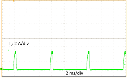
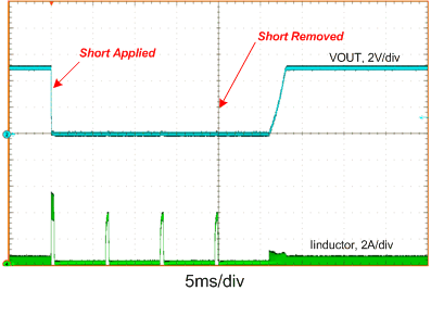
If the converter keeps triggering valley current limit for more than about 64 clock cycles, the device turns off both high and low side switches for approximately 5.5 ms (see TW in Section 7.7. If the overload is still present after the hiccup time, another 64 cycles is counted, and the process is repeated. If the current limit is not tripped for two consecutive clock cycles, the counter is reset. Figure 8-5 shows the inductor current with a hard short on the output. The hiccup time allows the inductor current to fall to zero, resetting the inductor volt-second balance. This is the method used for short-circuit protection and keeps the power dissipation low during a fault. Of course the output current is greatly reduced in this condition (see Section 7.8. A typical short-circuit transient and recovery is shown in Figure 8-6.
 Figure 8-5 Inductor Current Bursts in Short Circuit
 Figure 8-6 Short-Circuit Transient and Recovery
The high-side current limit trips when the peak inductor current reaches IL-HS (see Section 7.5). This is a cycle-by-cycle current limit and does not produce any frequency or current foldback. It is meant to protect the high-side MOSFET from excessive current. Under some conditions, such as high input voltage, this current limit may trip before the low-side protection. The peak value of this current limit varies with duty cycle.
In FPWM mode, the inductor current is allowed to go negative. Should this current exceed INEG, the low side switch is turned off until the next clock cycle. This is used to protect the low-side switch from excessive negative current. When the device is in AUTO mode, the negative current limit is increased to about IZC (about 0 A). This allows the device to operate in DCM.
The LM53625/35-Q1 response to a short circuit is: Peak current limit prevents excessive peak current while valley current limit prevents excessive average inductor current. After a small number of cycles of valley current limit triggers, hiccup mode is activated.