ZHCSO42B December 2015 – July 2021 LM53625-Q1 , LM53635-Q1
PRODUCTION DATA
- 1 特性
- 2 应用
- 3 说明
- 4 Revision History
- 5 Device Comparison
- 6 Pin Configuration and Functions
- 7 Specifications
- 8 Detailed Description
-
9 Application and Implementation
- 9.1 Application Information
- 9.2
Typical Applications
- 9.2.1 General Application
- 9.2.2 Fixed 5-V Output for USB-Type Applications
- 9.2.3 Fixed 3.3-V Output
- 9.2.4 Adjustable Output
- 9.3 What to Do and What Not to Do
- 10Power Supply Recommendations
- 11Layout
- 12Device and Documentation Support
- 13Mechanical, Packaging, and Orderable Information
封装选项
请参考 PDF 数据表获取器件具体的封装图。
机械数据 (封装 | 引脚)
- RNL|22
散热焊盘机械数据 (封装 | 引脚)
- RNL|22
订购信息
8.3.1 RESET Flag Output
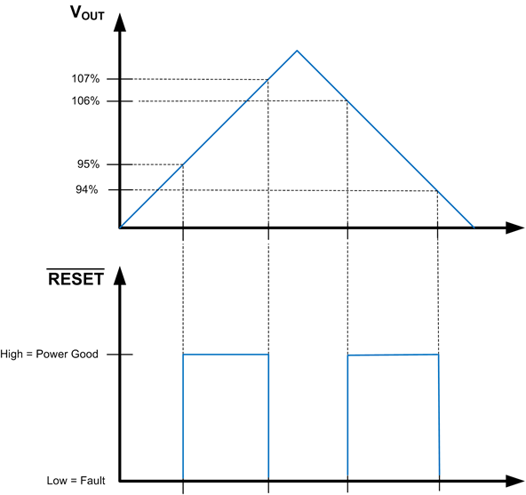
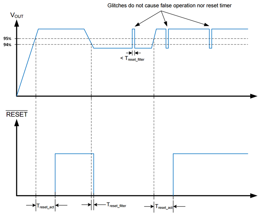
The RESET function, built into the LM53625/35-Q1, has special features not found in the ordinary Power-Good function. A glitch filter prevents false flag operation for short excursions in the output voltage, such as during line and load transients. Furthermore, there is a delay between the point at which the output voltage is within specified limits and the flag asserts Power Good. Because the RESET comparator and the regulation loop share the same reference, the thresholds track with the output voltage. This allows the LM53625/35-Q1 to be specified with a 96.5% maximum threshold, while at the same time specifying a 94 % worst case threshold with respect to the actual output voltage for that device. This allows tighter tolerance than is possible with an external supervisor device. The net result is a more accurate Power-Good function while expanding the system allowance for transients, and so forth. RESET operation can best be understood by reference to Figure 8-2 and Figure 8-3. The values for the various filter and delay times can be found in Section 7.7. Output voltage excursions lasting less than TRESET-filter do not trip RESET. Once the output voltage is within the prescribed limits, a delay of TRESET-act is imposed before RESET goes high.
This output consists of an open-drain NMOS; requiring an external pullup resistor to a suitable logic supply. It can also be pulled up to either VCC or VOUT, through an appropriate resistor, as desired. The pin can be left floating or grounded if the RESET function is not used in the application. When EN is pulled low, the flag output isl also be forced low. With EN low, RESET remains valid as long as the input voltage is ≥ 1.5 V. The maximum current into this pin should be limited to 10 mA, while the maximum voltage must be less than 8 V.
 Figure 8-2 Static
RESET Operation
 Figure 8-3 RESET
Timing Behavior
Figure 8-3 RESET
Timing BehaviorWhile the LM53625/35-Q1 reset function resembles a standard Power-Good function, its functionality is designed to replace a discrete reset device, reducing additional component cost. There are three major differences between the reset function and the normal power good function seen in most regulators.
- A delay has been added for release of reset. See Figure 8-2 and Figure 8-3 for more detail.
- RESET Output signals a fault (pulls its output to ground) while the part is disabled.
- RESET Continues to operate with input voltage as low as 1.5 V. Below this input voltage, RESET Output may be high impedance.
The threshold voltage for the RESET function is specified taking advantage of the availability of the LM53625/35-Q1 internal feedback threshold to the RESET circuit. This allows a maximum threshold of 96.5% of selected output voltage to be specified at the same time as 96 % of actual set point. The net result is a more accurate reset function while expanding the system allowance for transient response without the need for extremely accurate internal circuitry.