ZHCSO42B December   2015  – July 2021 LM53625-Q1 , LM53635-Q1

PRODUCTION DATA  

  1. 特性
  2. 应用
  3. 说明
  4. Revision History
  5. Device Comparison
  6. Pin Configuration and Functions
  7. Specifications
    1. 7.1 Absolute Maximum Ratings
    2. 7.2 ESD Ratings
    3. 7.3 Recommended Operating Conditions
    4. 7.4 Thermal Information
    5. 7.5 Electrical Characteristics
    6. 7.6 System Characteristics
    7. 7.7 Timing Characteristics
    8. 7.8 Typical Characteristics
  8. Detailed Description
    1. 8.1 Overview
    2. 8.2 Functional Block Diagram
      1. 8.2.1 Control Scheme
    3. 8.3 Feature Description
      1. 8.3.1 RESET Flag Output
      2. 8.3.2 Enable and Start-Up
      3. 8.3.3 Soft-Start Function
      4. 8.3.4 Current Limit
      5. 8.3.5 Hiccup Mode
      6. 8.3.6 Synchronizing Input
      7. 8.3.7 Undervoltage Lockout (UVLO) and Thermal Shutdown (TSD)
      8. 8.3.8 Input Supply Current
    4. 8.4 Device Functional Modes
      1. 8.4.1 AUTO Mode
      2. 8.4.2 FPWM Mode
      3. 8.4.3 Dropout
      4. 8.4.4 Input Voltage Frequency Foldback
    5. 8.5 Spread-Spectrum Operation
  9. Application and Implementation
    1. 9.1 Application Information
    2. 9.2 Typical Applications
      1. 9.2.1 General Application
        1. 9.2.1.1 Design Requirements
        2. 9.2.1.2 Detailed Design Procedure
          1. 9.2.1.2.1 External Components Selection
            1. 9.2.1.2.1.1 Input Capacitors
              1. 9.2.1.2.1.1.1 Input Capacitor Selection
            2. 9.2.1.2.1.2 Output Inductors and Capacitors Selection
              1. 9.2.1.2.1.2.1 Inductor Selection
              2. 9.2.1.2.1.2.2 Output Capacitor Selection
          2. 9.2.1.2.2 Setting the Output Voltage
            1. 9.2.1.2.2.1 FB for Adjustable Versions
          3. 9.2.1.2.3 VCC
          4. 9.2.1.2.4 BIAS
          5. 9.2.1.2.5 CBOOT
          6. 9.2.1.2.6 Maximum Ambient Temperature
        3. 9.2.1.3 Application Curves
      2. 9.2.2 Fixed 5-V Output for USB-Type Applications
        1. 9.2.2.1 Design Requirements
        2. 9.2.2.2 Detailed Design Procedure
        3. 9.2.2.3 Application Curves
      3. 9.2.3 Fixed 3.3-V Output
        1. 9.2.3.1 Design Requirements
        2. 9.2.3.2 Detailed Design Procedure
        3. 9.2.3.3 Application Curves
      4. 9.2.4 Adjustable Output
        1. 9.2.4.1 Design Requirements
        2. 9.2.4.2 Detailed Design Procedure
        3. 9.2.4.3 Application Curves
    3. 9.3 What to Do and What Not to Do
  10. 10Power Supply Recommendations
  11. 11Layout
    1. 11.1 Layout Guidelines
    2. 11.2 Layout Example
  12. 12Device and Documentation Support
    1. 12.1 Device Support
      1. 12.1.1 第三方米6体育平台手机版_好二三四免责声明
    2. 12.2 Documentation Support
      1. 12.2.1 Related Documentation
    3. 12.3 接收文档更新通知
    4. 12.4 支持资源
    5. 12.5 Trademarks
    6. 12.6 Electrostatic Discharge Caution
    7. 12.7 术语表
  13. 13Mechanical, Packaging, and Orderable Information

封装选项

请参考 PDF 数据表获取器件具体的封装图。

机械数据 (封装 | 引脚)
  • RNL|22
散热焊盘机械数据 (封装 | 引脚)
订购信息

Enable and Start-Up

Start-up and shutdown of the LM53625/35-Q1 are controlled by the EN input. Applying a voltage of ≥ 2 V activates the device, while a voltage of ≤ 0.8 V is required to shut it down. The EN input may also be connected directly to the input voltage supply. This input must not be left floating. The LM53625/35-Q1 utilizes a reference-based soft start that prevents output voltage overshoots and large inrush currents as the regulator is starting up. A typical start-up waveform is shown in Figure 8-4 along with timing definitions.

The waveforms shown in Figure 8-4 indicate the sequence and timing between the enable input and the output voltage and RESET. From the figure we can define several different start-up times depending on what is relevant to the application. Table 8-1 lists some definitions and typical values for the timings.
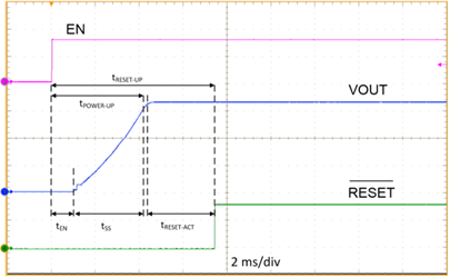
GUID-EA0B1B59-4BFF-4C6B-816D-0B945BA21552-low.pngFigure 8-4 Typical Start-up Waveform
Table 8-1 Typical Start-up Times
PARAMETERDEFINITIONVALUEUNIT
tRESET-READYTotal start-up sequence timeTime from EN to RESET released7.5ms
tPOWER-UPStart-up timeTime from EN to 90% of VOUT4ms
tSSSoft-start timeRise time of VOUT from 10% to 90%3.2ms
tENDelay timeTime from EN to start of VOUT rising1ms
tRESET-ACTRESET timeTime from output voltage within 94% and RESET released3ms