ZHCSEP3B February 2016 – February 2016 THS3217
PRODUCTION DATA.
- 1 特性
- 2 应用
- 3 说明
- 4 修订历史记录
- 5 Device Comparison Table
- 6 Pin Configuration and Functions
-
7 Specifications
- 7.1 Absolute Maximum Ratings
- 7.2 ESD Ratings
- 7.3 Recommended Operating Conditions
- 7.4 Thermal Information
- 7.5 Electrical Characteristics: D2S
- 7.6 Electrical Characteristics: OPS
- 7.7 Electrical Characteristics: D2S + OPS
- 7.8 Electrical Characteristics: Midscale (DC) Reference Buffer
- 7.9 Typical Characteristics: D2S + OPS
- 7.10 Typical Characteristics: D2S Only
- 7.11 Typical Characteristics: OPS only
- 7.12 Typical Characteristics: Midscale (DC) Reference Buffer
- 7.13 Typical Characteristics: Switching Performance
- 7.14 Typical Characteristics: Miscellaneous Performance
- 8 Parameter Measurement Information
-
9 Detailed Description
- 9.1 Overview
- 9.2 Functional Block Diagram
- 9.3 Feature Description
- 9.4 Device Functional Modes
-
10Application and Implementation
- 10.1
Application Information
- 10.1.1
Typical Applications
- 10.1.1.1 High-Frequency, High-Voltage, Dual-Output Line Driver for AWGs
- 10.1.1.2 High-Voltage Pulse-Generator
- 10.1.1.3 Single-Supply, AC-Coupled, Piezo Element Driver
- 10.1.1.4 Output Common-Mode Control Using the Midscale Buffer as a Level Shifter
- 10.1.1.5 Differential I/O Driver With independent Common-Mode Control
- 10.1.1
Typical Applications
- 10.1
Application Information
- 11Power Supply Recommendations
- 12Layout
- 13器件和文档支持
- 14机械、封装和可订购信息
9 Detailed Description
9.1 Overview
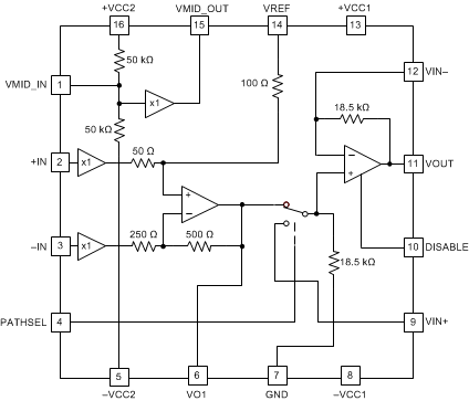
The THS3217 is a differential-input to single-ended output amplifier system that provides the necessary functional blocks to convert a differential output signal from a wideband DAC to a dc-coupled, single-ended, high-power output signal. The THS3217 typically operates using balanced, split supplies. Signal swings through the device can be adjusted around ground at several points within the device. Single-supply operation is also supported an ac-coupled signal path. The THS3217 supply voltage ranges from ±4.0 V to ±7.9 V. The two internal logic gates rely on a logic reference voltage at pin 7 that is usually tied to ground for any combination of power-supply voltages. The DISABLE control (pin 10) turns the output power stage (OPS) off to reduce power consumption when not in use.
A differential-to-single-ended stage (D2S) provides a high input impedance for a high-speed DAC (plus any reconstruction filter between the DAC and THS3217) operating over a common-mode input voltage range from –1 V to +3.0 V. This range is intended to support either current sourcing or current sinking DACs. The D2S is internally configured to reject the input common-mode voltage and convert the differential inputs to a single-ended output at a fixed gain of 2 V/V (6 dB).
An uncommitted, on-chip, wideband, unity-gain buffer is provided (between pins 1 and 15) to drive the VREF pin. The buffer offers extremely broad bandwidth to achieve very-low output impedance to high frequencies (Figure 51). The buffer does not provide a high full-power bandwidth because of a relatively low slew rate. The buffer stage includes a default midsupply bias resistor string of 50-kΩ each to set the default input to midsupply. This 25-kΩ Thevinin impedance is easily overridden with an external input source, but is intended to provide a midsupply bias for single-supply operation. The buffer amplifier that drives the VREF pin has two functions:
- Provides an easy-to-interface, dc-correction, servo-loop input
- Can be used as an offset injection point for the D2S output
The final OPS provides one of the highest-performance, current-feedback amplifiers available for line-driving applications. The 950-MHz SSBW stage provides 5000 V/μs of slew-rate, sufficient to drive a 5-VPP output with 500-MHz bandwidth. In addition, the OPS is able to drive a very-high continuous and peak output current sufficient to drive the most demanding loads at very high speeds. A unique feature added to the OPS is a 2 × 1 input multiplexer at the noninverting input. The PATHSEL control (pin 4) is used to select the appropriate signal path to the OPS noninverting input. One of the multiplexer select paths passes the internal D2S output directly to the OPS. The other select path accepts an external input to the OPS at VIN+ (pin 9). This configuration allows the D2S output, available at VO1 (pin 6), to pass through an external RLC filter and back into the OPS at VIN+ (pin 9).
If the OPS does not require power for certain application configurations, a shutdown feature has been included to reduce power consumption. For designs that do not use the OPS at all, two internal fixed resistors are included to define the operating points for the disabled OPS. An approximate 18.5-kΩ resistor to the logic reference (pin 7) from VIN+ (pin 9), and an approximate 18.5-kΩ, fixed, internal feedback resistor are included to hold the OPS pin voltages in range if no external resistors are used around the OPS. These resistors must be included in the design calculations for any external network.
Two sets of power supply-pins have been provided for both the positive and negative supplies. Pin 5 (–VCC2) and pin 16 (+VCC2) power the D2S and midscale buffer stages, while pin 8 (–VCC1) and pin 13 (+VCC1) supply power to the OPS. The supply rails are connected internally by antiparallel diodes. Externally, connect power first to the OPS, then connect back on each side with a π-filter (ferrite bead + capacitor) to the input-stage supply pins (see Figure 90). Do not use mismatched supply voltages on either the positive or negative sides because the supplies are internally connected through the antiparallel diodes. Imbalanced positive and negative supplies are acceptable, however.
When the OPS is disabled, the output pin goes to high impedance. However, do not connect two OPS outputs from different devices together and select them as a wired-or multiplexer. Although the high-impedance output is disabled, the inverting node is still available through the feedback resistor, and can load the active signal. The signal path through the inverting node typically degrades the distortion on the desired active signal in a wired-or multiplexer configuration using CFA amplifiers.
9.2 Functional Block Diagram
9.3 Feature Description
9.3.1 Differential to Single-Ended Stage (D2S) With Fixed Gain of 2-V/V (Pins 2, 3, 6 and 14)
This buffered-amplifier stage isolates the DAC output nodes from the differential to single-ended conversion. Presenting two high-impedance inputs allows the DAC to operate in its best configuration independent of subsequent operations. The two very wideband input buffers hold an approximately constant response shape over a wide input common-mode operating voltage. Figure 13 shows 6 dB of gain with 0.5-dB flatness through 500 MHz over the intended –1-to +3-V input common-mode range. In this case, the VREF pin is grounded, forcing the D2S output to be centered on ground for any input common-mode voltage. For the D2S-only tests, a 100-Ω load is used to showcase the performance of this stage directly driving a doubly-terminated cable. The wide input common-mode range of the D2S satisfies the required compliance voltage over a wide range of DAC types. Most current sourcing DACs require an average dc compliance voltage on their outputs near ground. Current sinking DACs require an average dc compliance voltage near their positive supply voltage for the analog section. The 3-V maximum common-mode range is intended to support DAC supplies up to 3.3 V, where the average output operating current pulls down from 3.3 V by the termination impedance from the supply. For instance, a 20-mA tail current DAC must level shift from a 3.3-V bias on the output resistors down to 3 V or lower. This DAC-to-THS3217 configuration requires at least a 300-mV dc level shift with half the tail current in each side, implying a 30-Ω load impedance to the supply on each side of the 20-mA reference current.
The overriding limits to the input common-mode operating range are due to the input buffer headroom. Over temperature, the D2S input headroom specification is 2 V to the negative supply and 1.5 V to the positive supply. Therefore, operation at a 3-V input common-mode voltage requires at least a 4.5-V positive supply, where 5 V is a more conservative minimum.
While DAC outputs rarely have any common-mode signal present (unless the reference current is being modulated), the D2S does a reasonable job of rejecting input common-mode signals over frequency. Figure 17 shows the CMRR to decrease above 10 MHz. For current-sinking DACs coming from a positive supply voltage, any noise on the positive supply looks like an input common-mode signal. Keeping the noise small at higher frequencies reduces the possibility of feedthrough to the D2S output due to the decreasing CMRR at higher frequencies. A current-sinking DAC uses pull-up resistors to the voltage supply to convert the DAC output current to a voltage. Make sure that the DAC voltage supply has been properly decoupled through a ferrite bead and capacitor, π-filter network similar to the supply decoupling for the THS3217 shown in Figure 90.
The D2S provides a differential gain of 6 dB. The gain is reasonably precise using internal resistor matching with extremely low gain drift over temperature (see Figure 61 and Figure 62). The single-ended D2S output signal can be placed over a wide range of dc offset levels using the VREF pin. The VREF pin shows a precise gain of 1 V/V to the D2S output. Grounding VREF places the first stage output centered on ground (with some offset voltage). For best ac performance through the D2S, anything driving the VREF pin must have a very wide bandwidth with very low output impedance over frequency while driving a 150-Ω load. The on-chip midscale buffer provides these features (see Figure 51). When a dc offset (or other small-level ac signal) must be applied to the VREF pin, buffer the signal through the midscale buffer stage. Maintain the total range of the dc offset plus signal swing within the available output swing range of the D2S. The headroom to the supplies is a symmetric ±1.65 V (max) over temperature. Therefore, on the minimum ±4-V supply, the D2S operates over a ±2.35-V output range. At the maximum ±7.9-V supply, a ±6.25-V output range is supported. At the higher swings, account for available linear output current, including the current into the internal feedback resistor load of approximately 500-Ω.
Figure 76 shows the internal structure of the D2S functional block. It consists of two internal stages:
- The first stage consists of two wideband, closed-loop, fixed gain of 1 V/V buffers to isolate the requirements of the complementary DAC output from the difference operation of the D2S.
- The second stage is a wideband CFA configured as a difference amplifier, operating in a fixed gain of 2 V/V, performing the differential to single-ended conversion.
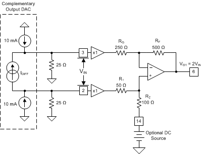 Figure 76. D2S Operating Example
The CFA design offers the best, full-power bandwidth versus supply current, with moderate noise and dc precision. Figure 76 shows a typical current-sourcing DAC with a 20-mA total tail current. The tail current is split equally between the 25-Ω termination resistors to produce a dc common-mode voltage and a differential ac current signal. This example sets the input common-mode voltage at 0.25 V, and is also the compliance voltage of the DAC. The 25-Ω termination resistors shown here are typically realized as a 50-Ω matched reconstruction (or Nyquist) filter between the DAC and the THS3217 buffer inputs for most AWG applications. The DAC signal is further amplified by 6 dB in the second stage for a net transimpedance gain of 100-Ω to the D2S output at VO1. This configuration produces a 2-VPP output for the 20-mA reference current assumed in the example of Figure 76. The input common-mode voltage is cancelled on the two sides of the op amp circuit to give a ground referenced output. Any voltage applied to the VREF pin has a gain transfer function of 1 V/V to VO1, independent of the signal path, as long as the source impedance of VREF is very low at dc and over frequency.
The IN+ buffer output drives a 150-Ω load with VREF grounded. Any source driving VREF must have the ability to drive a 150-Ω load with low output impedance across frequency. For differential input signals, the IN– buffer drives a 150-Ω active load. The active load is realized by a combination of the 250-Ω RG resistor and the inverted and attenuated signal present at the inverting terminal of the difference amplifier stage. If only IN– is driven (with IN+ at a dc fixed level), the load is 250 Ω.
The resistor values around the D2S difference amplifier are derived in the following sequence, as shown in Figure 77:
- Select the feedback resistor value to set the response shape for the wideband CFA stage. The 500-Ω design used here was chosen as a compromise between loading and noise constraints.
- Set the input resistor on the inverting input side to give the desired single-sided gain for that path. Setting RG= 250-Ω results in a gain of –2 V/V from the buffered signal (–V) to the output of the difference amplifier.
- Solve the required attenuation to the noninverting input to get a matched gain magnitude for the signal provided at the buffer output (+V) on the noninverting path. If α = R2 / (R1 + R2), as shown in Figure 77, then the solution for α is shown in Equation 2:
- After solving the attenuation from the buffer output to the amplifier noninverting input, set the impedance (R1 + R2). It is preferable to have the two first stage buffer outputs drive the same load impedance to match nonlinearity in their outputs in order to improve even-order harmonic distortion. The load impedance from –V to RG has an active impedance because of the inverted and attenuated version of the input signal appearing at the inverting amplifier node from the +V input signal. Assuming a positive input signal into the +V path, an attenuated version of the signal appears at the amplifier summing junction side of RG, while the inverted version of the signal appears on the input side of RG.


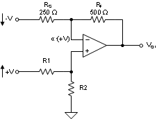 Figure 77. D2S Impedance Analysis
The impedance seen at node –V in Figure 77 is derived in Equation 3 by solving for the V/I expression across RG.

For load balancing, (R1 + R2) = 150 Ω while the attenuation is α. More generally, all the terms are now available to solve for R2, as shown in Equation 4:

R1 is then simply (Zi- R2) = 50 Ω.
This analysis for matched gains and buffer loads can be applied to a more general discrete design using different target gains and starting RF values. It is clearly useful to have the attenuation and buffer loading accurately controlled. Therefore, it is very important to control the impedance at the VREF pin to be as low as possible. For instance, using the midscale buffer to drive the VREF pin only adds 0.21 Ω dc impedance in series with R2. This low dc output impedance can only be delivered with a closed-loop buffer design. For discrete implementations of this D2S, consider the BUF602 buffer and LMH6702 wideband CFA amplifier. For even better dc and ac output impedance in the buffers (and possibly better gain), use a closed-loop, dual, wideband op amp like the OPA2889 for lower frequency applications, or the OPA2822 for higher frequency. These unity gain stable op amps can be used as buffers offering different performance options along with the LMH6702 wideband CFA over the design point chosen for the THS3217.
After gain matching is achieved in the single op amp differential stage, the common-mode input voltage is cancelled to the output, and the VREF input voltage is amplified by 1 V/V to the output. The analysis circuit is shown in Figure 78, where VREF is shown grounded at the R2 element.
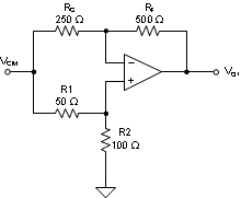 Figure 78. D2S Common-Mode Cancellation
The gain magnitudes are equal on each side of the differential inputs; therefore, the common-mode inputs achieve the same gain magnitude, but opposite phase, resulting in common-mode signal cancellation. The inverting path gain is VCM × (RF / RG). The noninverting path gain is VCM × α × (1 + RF / RG). Using Equation 5:

the noninverting path gain becomes +VCM × RF / RG, and adding that result to the inverting path signal cancels to zero. Slight gain mismatches reduce this rejection to the 55-dB typical CMRR, with a 47-dB tested minimum. The 47-dB minimum over the 3-V maximum common mode input range adds another ±13.4-mV worst-case D2S output offset term to the specified maximum ±35-mV output offset with 0-V input common-mode voltage. The polarity of the gain mismatch is random.
The VREF pin input voltage (VREF) generates a gain of 1 V/V using the analysis shown in Figure 79
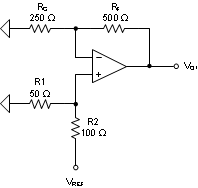 Figure 79. Gain Transfer Function from VREF to VO1
The gain from VREF to VO1 is shown in Equation 6:

Getting both R1 and (R1 + R2) in terms of RG and the target attenuation, α simplifies, as shown in Equation 7:

Putting Equation 7 back into the gain expression(Equation 6), and expanding out gives:

Recall that in order to get differential gain balance, α = –(RF / RG). Putting that into Equation 8 reduces the expression to VO1 = VREF, a gain of 1 V/V. This gain is very precise as shown in the D2S Electrical Characteristics table, where the tested dc limits are 0.985 V/V to 1.015 V/V.
The D2S output offset and drift are largely determined by the internal elements. The only external consideration is the dc source impedance at the two buffer inputs. With low source impedance, the D2S output offset is tested to be within ±35 mV, that becomes a maximum ±17 mV input differential offset specification. Assuming the dc source impedances are closely matched, the mismatch in the two input bias currents adds another input offset term for higher source impedances. The input bias offset current is limited in test to be < ±0.40 µA. This error term does not rise to add more than ±1 mV input differential offset until the dc source impedance exceeds 2.5 kΩ. A high dc source impedance most commonly occurs in an input ac-coupled, single-supply application, where dc offsets are less critical.
The absolute input bias currents modifies the common-mode input voltage if the dc source resistance is too large. That term is tested to a limit of ±4 µA on each input. To move the input common mode voltage by ±100 mV, the dc source impedance must exceed 25 kΩ. This added input common-mode voltage is cancelled by the D2S at the output (VO1, pin6).
The D2S output noise is largely fixed by the internal elements. The D2S shows a differential input voltage noise of 9 nV/√Hz, and a current noise of 2 pA/√Hz on each input. Higher termination resistors increase this source noise, as given by Equation 9, where Rt is the dc termination impedance at each buffer input. The D2S has a 1/f corner at approximately 30 kHz (see Figure 18).

The total differential input noise is dominated by the differential voltage noise. For instance, evaluating this expression for Rt = 200 Ω on each input, increases the total differential input noise to 9.4.nV/√Hz, only slightly greater than the 9 nV/√Hz for the D2S with 0-Ω source Rt on each input. If higher final output SNR is desired, consider generating as much input swing as the DAC can support, but increase the termination impedance. It is possible that a lower tail current with higher Rt will yield improved SNR at the D2S input. This differential input noise appears at the D2S output times a gain of 2 V/V.

9.3.2 Midscale (DC) Reference Buffer (Pin 1 and Pin 15)
This optional block can be completely unconnected and not used if the design does not require this feature. Internal 50-kΩ resistors to the power supplies bias the input of the buffer to the midpoint of the supplies used. The internal resistors set a midsupply operating point when the buffer is not used, as well as a default midsupply point at the buffer output to be used in other stages for single-supply, ac-coupled applications.
The buffer provides a very wideband, low output-impedance when used to drive the VREF pin (see Figure 51). To provide this low broadband impedance, the closed-loop midscale (dc) reference buffer offers a very broadband SSBW, but only a modest large-signal bandwidth (LSBW); see Figure 49. This path is not normally intended to inject a wideband signal, but can be used for lower-amplitude signals. Driving the buffer output into the VREF pin allows a wideband small-signal term to be added into the D2S along with the signal from the differential inputs.
The midscale (or dc) reference buffer injects an offset voltage to the output offset of the D2S when it drives the VREF pin. The offset has very low drift, but consider the effect of the input bias current times the dc source impedance at VMID_IN (pin 1). When used as a default midsupply reference for single-supply operation, the input to this buffer is just the average of the total power supplies though a 25-kΩ source impedance. Add an external capacitor to filter the supply and the 50-kΩ internal resistors. A 1-µF capacitor on pin 1 adds a 6-Hz pole to the noise sources. If lower noise at lower frequencies is required, implement a midscale divider with external, lower-valued resistors in parallel with the internal 50-kΩ values.
If the midscale buffer drive the VREF pin, another noise term is added to Equation 9 and Equation 10. The midscale buffer 4.4-nV/√Hz voltage noise is amplified by 0 dB, and adds (RMS) a negligible impact to the total D2S output noise. The biggest impact comes when the internal default 50-kΩ dividers are used. Be sure to decouple pin 1 with at least a 1-µF capacitor in the application to reduce the noise contribution through this path. Figure 80 is the simulation circuit where the only change is to add or remove the 1-µF capacitor.
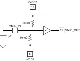 Figure 80. Midscale Buffer Noise Model
Figure 81 shows the simulated output noise for the midscale buffer using the internal 50-kΩ divider with and without a 1-µF capacitor on pin 1.
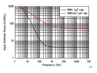 Figure 81. Buffer-Output Noise Comparison With and Without the 1-µF Bypass Capacitor on Pin 1
In the flat region, the 1-µF capacitor reduces the midscale buffer output spot noise from approximately 55 nV/√Hz to 4.4 nV/√Hz. If the noise below 100 Hz is unacceptable, either add a low-noise buffer to drive this input, or add lower-value resistors externally to set up the midsupply bias. Also, consider the noise impact of any reference voltage source driving the midscale buffer path.
9.3.3 Output Power Stage (OPS) (Pins 4, 7, 9, 10, 11, and 12)
This wideband current-feedback amplifier (CFA) provides a flexible output driver with several unique features. The OPS can be left unused if the specific application only uses the D2S alone, or a combination of the D2S with an off-chip power driver. If left unused, simply tie DISABLE (pin 10) and PATHSEL (pin 4) to the positive supply. This logic configuration turns the OPS off and opens up the external and internal OPS noninverting input paths. An internal fixed 18.5-kΩ resistor holds the external input pin at the logic reference voltage on pin 7. Additionally, the OPS output is connected to the inverting input through another internal 18.5-kΩ resistor when no external resistors are installed on pins 9, 11, or 12. Disabling the OPS saves approximately 21 mA of supply current from the nominal total 54 mA with all stages operating on ±6-V supplies.
The noninverting input to the OPS provides two possible paths controlled by the PATHSEL logic control, pin 4. With the logic reference (pin 7) at ground, floating pin 4 or controlling it to a voltage < 0.7 V connects the input path directly to the internal D2S output. Tying pin 4 to the positive supply, or controlling it to a logic level > 1.3 V, connects the input path to the external input at pin 9. The intent for this switched input is to allow an external filter to be inserted between the D2S output and OPS inputs when needed, and bypass the filter when not. Alternatively, this switched input also allows a completely different signal path to be inserted at the OPS input, independent of that available at the internal D2S output.
In situations where the D2S output at pin 6 is switched into another off-chip power driver, the OPS can be disabled using pin 10. With the logic reference (pin 7) at ground, floating pin 10, or controlling it to a voltage < 0.7 V, enables the OPS. Tying pin 10 to the positive supply, or controlling it to a logic level > 1.3 V, disables the OPS.
Operation of the wideband, current-feedback OPS requires an external feedback resistor and a gain element. After configuring, the OPS can amplify the D2S output through either the noninverting path, or be configured as an inverting amplifier stage using the external OPS input at pin 9 as a dc reference.
One of the first considerations when designing with the OPS is determining the external resistor values as a function of gain in order to hold the best ac performance. The loop gain (LG) of a CFA is set by the internal open-loop transimpedance gain from the inverting error current to the output, and the effective feedback impedance to the inverting input. The nominal internal open-loop transimpedance gain and phase are shown in Figure 82.
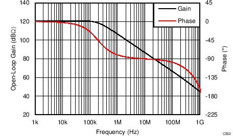 Figure 82. Simulated OPS ZOL Gain And Phase
The feedback transimpedance (ZOPT) can be approximated as shown in Equation 11, where Ri is the open-loop, high-frequency impedance into the inverting node of the OPS. For a detailed derivation of Equation 11, see Setting Resistor Values to Optimize Bandwidth section in the OPA695 datasheet (SBOS293).

As the signal gain is varied, hold ZOPT approximately constant to hold the ac response constant over gain. Holding ZOPT constant is a requirement to solve for RF. An example of the THS3217 OPS RF derivation is shown in Equation 12:

The calculations are complicated by the internal feedback resistor value of approximately 18.5-kΩ. After the external RF is approximately set by the constant bandwidth consideration, the RG must be set considering the other gain error terms. From the noninverting input of a CFA op amp, the total gain to the output includes a loss through the input buffer stage (described by the CMRR) and the loop gain (LG) loss set by the typical dc open-loop transimpedance gain and the feedback transimpedance. Extract the buffer gain from the VIN+ input to the VIN– input from the CMRR using Equation 13. This gain loss only applies to the noninverting mode of operation and can be neglected in inverting mode operation.

The OPS has a typical CMRR of 49 dB (buffer gain, β = 0.9965) with a tested minimum of 47 dB (minimum buffer gain of 0.9955). The dc LG adds to the gain error. The LG is given by Equation 14 where the typical design gain of 2.5 V/V value is also shown (the 245 Ω shown for RF is the external 249-Ω feedback resistor in parallel with the internal 18.5-kΩ feedback resistor).

The closed-loop output impedance with a heavy load also adds a minor gain loss that is neglected here. The total noninverting gain is then set by Equation 15 (remember to include the internal RF in this analysis. The RF’ shown here is the parallel combination of the internal and external feedback resistors).

Using nominal values for each term at the specified RF = 249 Ω and RG = 162 Ω gives the gain calculation in Equation 16, yielding a nominal gain very close to 2.5 V/V.

Testing the total gain spread with the internal variation in buffer gain, open-loop transimpedance gain, internal feedback resistor, and ±1% external resistor variation gives a worst-case gain spread of 2.49 V/V to 2.51 V/V. The gain error is primarily dominated by the external 1% resistors. For the tighter tolerance shown in Table 2, use 0.1% precision resistors.
At very low gains (< 1.5 V/V) parasitic LC effects at the inverting input render a flat frequency response impossible. Looking then at gains from 1.5 V/V and up, a table of nominally recommended RF and RG values is shown in Table 2. Do not operate the OPS in noninverting gains of less than 2.5 V/V for large output signals because the limited slew-rate of the CFA input buffer causes signal degradation. Table 2 accounts for the nominal gain losses described previously, and uses standardized resistor values to minimize the nominal gain-error to target gain. The calculation also restricts the solution to a minimum RG = 20 Ω. The gain calculations include the nominal buffer gain loss, the loop-gain effect, and the nominal internal feedback resistor = 18.5 kΩ.
Table 2. Optimized RF Values for Different OPS Noninverting Signal Gains
| TARGET GAIN (V/V) | MEASURED SSBW (MHz) | BEST RF
(Ω) |
BEST RG
(Ω) |
CALCULATED GAIN | GAIN ERROR (%) | |
|---|---|---|---|---|---|---|
| (V/V) | (dB) | |||||
| 1.5 | 1400 | 294 | 562 | 1.505 | 3.551 | 0.3 |
| 2 | — | 274 | 267 | 1.998 | 6.013 | –0.1 |
| 2.5 | 950 | 249 | 162 | 2.500 | 7.960 | 0 |
| 3 | — | 232 | 113 | 3.008 | 9.566 | 0.3 |
| 3.5 | — | 205 | 80.6 | 3.493 | 10.863 | –0.2 |
| 4 | — | 182 | 59 | 4.028 | 12.103 | 0.7 |
| 4.5 | — | 165 | 46.4 | 4.495 | 13.055 | –0.1 |
| 5 | 652 | 140 | 34.8 | 4.960 | 13.910 | –0.8 |
| 5.5 | — | 121 | 26.7 | 5.467 | 14.754 | –0.6 |
| 6 | — | 113 | 22.1 | 6.043 | 15.624 | 0.7 |
| 6.5 | — | 115 | 20.5 | 6.532 | 16.301 | 0.5 |
| 7 | — | 121 | 20 | 6.965 | 16.859 | –0.5 |
| 7.5 | — | 133 | 20 | 7.553 | 17.563 | 0.7 |
| 8 | — | 143 | 20 | 8.043 | 18.108 | 0.5 |
| 8.5 | — | 154 | 20 | 8.580 | 18.670 | 0.9 |
| 9 | — | 162 | 20 | 8.971 | 19.057 | –0.3 |
| 9.5 | — | 174 | 20 | 9.557 | 19.606 | 0.6 |
| 10 | 315 | 187 | 20.5 | 9.966 | 19.970 | –0.3 |
The measured bandwidths in Table 2 come from Figure 25 using the resistor values in the table and a 100-Ω load. Plotting the RF value versus gain gives the curve of Figure 83. The curve shows some ripple due to the standard value resistors used to minimize the target dc gain error.
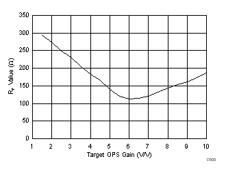 Figure 83. Suggested External RF Value vs Noninverting Gain for the OPS
Using RF values greater than the recommended values in Table 2 band-limits the response, whereas using less than the recommended RF values peaks the response. Using the values shown in Table 2 results in an approximately constant SSBW (see Figure 25. Holding a more constant loop-gain over the external gain setting also acts to hold a more constant output impedance profile, as shown in Figure 84. The swept-frequency, closed-loop, output impedance is shown for gains of 2.5 V/V, 5 V/V, and 10 V/V using the RF and RG values of Table 2. The first two steps do a good job of delivering the same (and very low) output impedance over frequency, while the gain of 10 V/V shows the expected higher closed-loop output impedance due to the reduced loop-gain and bandwidth.
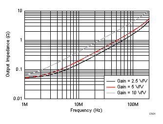 Figure 84. OPS Closed-Loop Output Impedance vs Gain Setting
Reducing the RF value with increasing gain also helps minimize output noise versus a fixed RF design. See Figure 39 for the three noise terms for the OPS. The total output noise calculation is shown in Equation 17:

where
- RS is the source impedance on the noninverting input. If the OPS is driven from the D2S stage directly using the internal path, RS ≈ 0 Ω.
- NG = (1 + RF / RG) for the design point.
- The flat-band noise numbers for the OPS are:
- Eni = 3.2 nV/√Hz
- Ibn = 2.7 pA/√Hz
- Ibi = 30 pA/√Hz
Using the values of RF and RG listed in Table 2, a swept gain output- and input-referred noise estimate is computed, as shown in Table 3. In this sweep, RS = 0 Ω. The input-referred noise (Eni) in Table 2 is at the noninverting input of the OPS. To refer the noise to the D2S differential inputs, divide the output noise by two if there is no interstage loss. Dividing the Eni column by 2 V/V shows that the OPS noise contribution is negligible when referred to the D2S inputs, where the 9-nV/√Hz differential input noise dominates. Operating with higher feedback resistors in the OPS quickly increases the output noise due to the inverting input current noise term. Although increasing RF improves phase margin (for example, when driving a capacitive load), be careful to check the total output noise using Equation 17.
Table 3. Total Input- and Output-Referred Noise of the OPS Versus Gain
| TARGET GAIN (V/V) |
BEST RF
(Ω) |
BEST RG
(Ω) |
EO
(nV/√Hz) |
Ein
(nV/√Hz) |
|---|---|---|---|---|
| 1.5 | 294 | 562 | 10.4 | 6.9 |
| 2 | 274 | 267 | 11.3 | 5.6 |
| 2.5 | 249 | 162 | 12.3 | 4.9 |
| 3 | 232 | 113 | 13.5 | 4.5 |
| 3.5 | 205 | 80.6 | 14.7 | 4.2 |
| 4 | 182 | 59 | 15.9 | 4.0 |
| 4.5 | 165 | 46.4 | 17.2 | 3.8 |
| 5 | 140 | 34.8 | 18.6 | 3.7 |
| 5.5 | 121 | 26.7 | 20.0 | 3.6 |
| 6 | 113 | 22.1 | 21.4 | 3.6 |
| 6.5 | 115 | 20.5 | 22.9 | 3.5 |
| 7 | 121 | 20 | 24.4 | 3.5 |
| 7.5 | 133 | 20 | 25.9 | 3.5 |
| 8 | 143 | 20 | 27.4 | 3.4 |
| 8.5 | 154 | 20 | 29.0 | 3.4 |
| 9 | 162 | 20 | 30.5 | 3.4 |
| 9.5 | 174 | 20 | 32.1 | 3.4 |
| 10 | 187 | 20.5 | 33.6 | 3.4 |
Operating the OPS as an inverting amplifier is also possible. When driving the OPS directly from the D2S to the RG resistor, use the values shown in Table 2 for the noninverting mode to achieve good results. Note that the RG resistor is the load for the D2S stage. Operating with the D2S driving an RG < 80 Ω increases the harmonic distortion of the D2S. In that case, scaling RF and RG up to reduce the loading may result in better system performance at the cost of a lower OPS bandwidth. Driving the D2S output at pin 6 into the OPS in an inverting mode allows for the option to select the external input of the OPS, and drive another signal or dc level into the noninverting input at pin 9. In order to reduce layout parasitics, consider splitting the RG resistor in two, with the first half close to pin 6 and the second half close to pin 12. Splitting RG in this manner places the trace capacitance inside the two resistors keeping both active nodes more stable. Also, open up the ground and power planes under the trace, if possible.
Using the PS to receive and amplify a signal in the inverting mode with a matched terminating impedance, requires another resistor to ground (RM) along with RG. This RM resistor is shown in Figure 85 for a 50-Ω matched input impedance design.
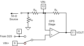 Figure 85. Inverting OPS Operation With Matched Input Impedance
Table 4 gives the recommended external resistor values versus gain for the inverting gain mode with input matching configuration. Table 4 solves for the required RF to simultaneously allow the gain, input impedance (50 Ω), and feedback transimpedance to be controlled to the optimum target values. The table includes the effect of the internal 18.5-kΩ feedback resistor, and minimizes the RMS error to input impedance target (ZI) and overall gain.
Table 4. Resistor Values Versus Gain for the Inverting OPS Configuration
| TARGET GAIN (V/V) |
MEASURED SSBW (MHz) |
BEST RF (Ω) | BEST RG (Ω) | BEST RM (Ω) | CALCULATED GAIN | GAIN ERROR (%) | ZI (Ω) | ZI ERROR (%) | |
|---|---|---|---|---|---|---|---|---|---|
| (V/V) | (dB) | ||||||||
| 1 | 1000 | 280 | 274 | 60.4 | 1.002 | 0.022 | 0.250 | 49.490 | –1.019 |
| 1.5 | — | 255 | 169 | 71.5 | 1.506 | 3.554 | 0.376 | 50.243 | 0.486 |
| 2 | — | 249 | 124 | 84.5 | 2.000 | 6.019 | –0.014 | 50.254 | 0.508 |
| 2.5 | 860 | 237 | 93.1 | 107 | 2.490 | 7.924 | –0.403 | 49.784 | –0.433 |
| 3 | — | 226 | 75 | 150 | 3.013 | 9.581 | 0.444 | 50.000 | 0.000 |
| 3.5 | — | 226 | 63.4 | 237 | 3.491 | 10.859 | –0.258 | 50.019 | 0.039 |
| 4 | — | 221 | 54.9 | 604 | 4.010 | 12.064 | 0.259 | 50.326 | 0.651 |
| 4.5 | — | 226 | 49.9 | Open | 4.525 | 13.111 | 0.545 | 49.90 | –0.200 |
| 5 | 760 | 249 | 49.9 | Open | 4.985 | 13.953 | –0.301 | 49.90 | –0.200 |
| 5.5 | — | 274 | 49.9 | Open | 5.485 | 14.784 | –0.264 | 49.90 | –0.200 |
| 6 | — | 301 | 49.9 | Open | 6.026 | 15.601 | 0.434 | 49.90 | –0.200 |
| 6.5 | — | 324 | 49.9 | Open | 6.486 | 16.240 | –0.208 | 49.90 | –0.200 |
| 7 | — | 348 | 49.9 | Open | 6.967 | 16.861 | –0.472 | 49.90 | –0.200 |
| 7.5 | — | 374 | 49.9 | Open | 7.487 | 17.487 | –0.167 | 49.90 | –0.200 |
| 8 | — | 402 | 49.9 | Open | 8.048 | 18.114 | 0.600 | 49.90 | –0.200 |
| 8.5 | — | 422 | 49.9 | Open | 8.448 | 18.536 | –0.607 | 49.90 | –0.200 |
| 9 | — | 449 | 49.9 | Open | 8.989 | 19.074 | –0.123 | 49.90 | –0.200 |
| 9.5 | — | 475 | 49.9 | Open | 9.509 | 19.563 | 0.100 | 49.90 | –0.200 |
| 10 | 260 | 499 | 49.9 | Open | 9.990 | 19.991 | –0.100 | 49.90 | –0.200 |
At higher gains, RM increases to larger values, and the resistor is excluded from the circuit. The resulting input impedance of the network is resistor RG. From that point, RF simply increases to get higher gains, thereby rapidly reducing the SSBW. However, below a gain of –5 V/V, the inverting design with the values shown in Table 4 holds a more constant SSBW versus the noninverting mode (see Figure 26).
9.3.3.1 Output DC Offset and Drift for the OPS
The OPS provides modest dc precision with typical and maximum dc error terms in Table 5. The input offset voltage applies to either input path with very little difference between the internal and external paths.
Table 5. Typical Offset and Bias Current Values for the OPS
| PARAMETER | TYPICAL | MINIMUM | MAXIMUM | UNIT |
|---|---|---|---|---|
| VIO | ±1 | –12 | 12 | mV |
| Ibn | 5 | –5 | 15 | µA |
| Ibi | ±5 | –40 | 40 | µA |
Selecting the internal path results in no source resistance for Ibn, so that term drops out. When the external path is selected, a dc source impedance may be present, so the Ibn term creates another error term, and adds to the total output offset.
Stepping through an example design for the OPS output dc offset using the external path with a low insertion loss filter shown in Figure 92, along with its RF and RG values, gives the following results:
- RS for the Ibn term = 34 Ω || 249 Ω = 30 Ω. (dc source impedance for the filter design)
- RF including the internal 18.5 kΩ resistor = 249 Ω || 18.5 kΩ = 245.7 Ω
- Resulting gain with the 130-Ω RG element = 2.89 V/V
Table 6 shows the typical and worst-case output error terms. Note that a positive current out of the noninverting input gives a positive output offset term, whereas a positive current out of the inverting input gives a negative output term.
Table 6. Output Offset Voltage Contribution From Various Error Terms at 25°C
| ERROR TERM | TYPICAL | MINIMUM | MAXIMUM | UNIT |
|---|---|---|---|---|
| Ibn × RS × AV | 0.433 | –0.43 | 1.29 | mV |
| VIO × AV | ±2.89 | –34.68 | 34.68 | mV |
| Ibi × RF | ±1.22 | –9.83 | 9.83 | mV |
| Total error | –3.67 to +4.54 | –44.94 | 45.8 | mV |
The input offset voltage dominates the error terms. The worst-case numbers are calculated by adding the individual errors algebraically, but is rarely seen in practice. None of the OPS input dc error terms are correlated. To compute output drift numbers, use the same gains shown in Table 6 with the specified drift numbers.
The OPS PATHSEL control responds extremely quickly with low-switching glitches, as shown in Figure 86. For this test, the D2S input is set to GND, and the output of the D2S is connected to the external OPS input. The PATHSEL switch is then toggled at 10 MHz. The results show the offset between the internal and external paths as well matched.
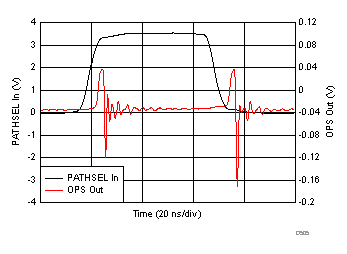 Figure 86. OPS Path-Select Switching Glitch
The OPS includes a disable feature that reduces power consumption from approximately 21 mA to 2.4 mA. The logic controls are intended to be ground-referenced regardless of the power supplies used. The logic reference (GND, pin 7) is normally grounded and also provides a connection to the internal 18.5-kΩ resistor on pin 9 (default bias to pin 7). Operating in a single-supply configuration with –VCC at GND and the external OPS input (pin 9) floated, places pin 9 internally at –VCC = GND. Driving the external OPS input (pin 9) from a source within the operating range overrides the bias to –VCC. However, if the application requires pin 9 to be floated in a single-supply operation, consider centering the voltage on pin 9 with an added 18.5-kΩ external resistor to the +VCC supply.
If the disable feature is not needed, simply float or ground DISABLE (pin 10) to hold the OPS in the enabled state. Increasing the voltage on the DISABLE pin greater than 1.3 V disables the OPS and reduces the current to approximately 2.4 mA. If the OPS is unused in the application, it can be disabled by tying pin 10 to +VCC, even up to the maximum operating supply of 15.8 V in a single-supply design.
Do not move the logic threshold away from those set by the logic ground at pin 7. If a different logic swing level is required, and pin 7 is biased to a different voltage, be sure the source can sink the typical 280 µA coming out of pin 7. Also recognize that the 18.5-kΩ bias resistor on the external OPS input (pin 9) is connected to pin 7 voltage internally.
As shown in Figure 56, the OPS enables in approximately 100 ns from the logic threshold at 1.0 V while disabling to a final value in approximately 500 ns.
9.3.3.2 OPS Harmonic Distortion (HD) Performance
The OPS in the THS3217 provides one of the best HD solutions available through high power levels and frequencies. Figure 31 and Figure 32 show the swept-frequency HD2 and HD3, where the second harmonic is clearly the dominant term over the third harmonic. Typical wideband CFA distortion is reported only through 2-VPP output while Figure 31 and Figure 32 provide sweeps at 5 VPP and 8 VPP into a 100-Ω load. These curves normally show a 20-dB per decade rise with frequency due to loop-gain roll-off. At the highest 8-VPP swing, the onset of slew rate limited HD is seen at approximately 40 MHz. The required output signal slew rate at 8 VPP and 40 MHz is 4 VPEAK × 2π × 40 MHz = 1000 V/µs. The output signal requires 1/5 of the available slew rate that will take the HD2 off the 20-dB per decade rate in the –50-dBc operating region shown. A slight shift in the HD3 slope is also seen around 40 MHz for 8-VPP output in Figure 32.
The distortion performance is extremely robust as a function of RLOAD (see Figure 33 and Figure 34). Normally, heavier loads degrade the distortion performance, as seen for the HD3 in Figure 34. However, the HD2 actually improves slightly going from a 200-Ω load to a 100-Ω load.
One of the key advantages offered by the CFA design in the OPS is that the distortion performance holds approximately constant over gain, as seen in the full-path distortion measurements of Figure 7 and Figure 8. Here, the D2S provides a fixed gain of 2 V/V driving a 200-Ω interstage load and using the internal path to drive the OPS at gains from 1.5 V/V to 10 V/V. Holding the loop-gain approximately constant by adjusting the feedback RF value with gain results in vastly improved performance versus a voltage-feedback-based design.
Testing a 5-VPP output from the OPS with the supplies swept from the minimum ±4 V to ±7.5 V in Figure 35 and Figure 36 show:
- The 1.5-V headroom on ±4-V supplies and ±2.5-V output voltage results in degraded performance. At the lower supplies, target lower output swings for improved linearity performance.
- The HD2 does not change significantly with supply voltages above ±5 V. The HD3 does improve slightly at higher supply-voltage settings.
From these plots at ±7.5-V supplies, a 5-VPP output into 100-Ω load shows better than –60-dBc HD2 and HD3 performance through 50 MHz. This exceptional performance is available with the OPS configured as a standalone amplifier. Combining this performance with the D2S stage (see Figure 3 and Figure 4) degrades the distortion due to the D2S and OPS harmonics combining in phase, and internal coupling between the stages. With the D2S and OPS running together at a final 5-VPP output and 50 MHz, the HD2 drops to –50 dBc, and HD3 to –58 dBc on ±6-V supplies. Lower output swings for the combined stages provide much lower distortion. The 2-VPP output curves on Figure 3 and Figure 4 show –57 dBc for HD2, and a remarkable –76 dBc for HD3 at 50 MHz.
9.3.3.3 Switch Feedthrough to the OPS
The OPS has two logic control pins, giving four combinations of states; therefore, various feedthrough effects must be considered. Figure 57 and Figure 58 show the feedthrough of the switches with the OPS disabled. With the OPS enabled, the signal feedthrough from the deselected input to the OPS output is shown in Figure 87 and Figure 88 at different closed-loop OPS gains. The results are shown for a 100-mVPP signal at the deselected input and are not normalized to the gain of the OPS. Adding a low-pass filter between the DAC and the D2S inputs helps reduce the feedthrough at higher frequencies.
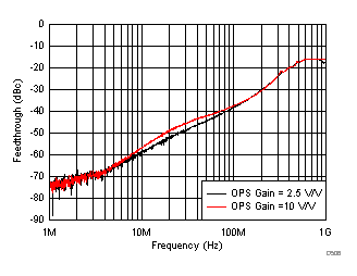
| PATHSEL < 0.7 V, | ||
| 100-mVPP signal to VIN (pin 9) |
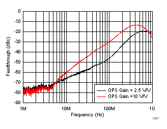
| PATHSEL > 1.3 V, | ||
| 100-mVPP signal to VREF (pin 14) with D2S inputs grounded |
9.3.3.4 Driving Capacitive Loads
The OPS can drive heavy capacitive loads very well as shown in Figure 43 to Figure 48. All high-speed amplifiers benefit from the addition of an external series resistor to isolate the load capacitor from the feedback loop. Not having the series isolation resistor often leads to response peaking and possibly oscillation. If frequency response flatness under capacitive load is the design goal, all CFA type amplifiers benefit by operating with slightly higher RF values. Targeting a slightly higher feedback transimpedance increases the nominal phase margin before the capacitive load acts to decrease it. Using a higher RF value has the effect of achieving good flatness across a range of capacitive loads using lower external series resistor values. Although the suggested RF and RG values of Table 7 apply when driving a 100-Ω load, if the intended load is capacitive (for example, a passive filter with a shunt capacitor as the first element, another amplifier, or a Piezo element), use the values reported in Table 7 as a starting point. The values in Table 7 were used to generate Figure 43 and Figure 44. The results come from a nominal total feedback transimpedance target of 405 Ω (versus 351 Ω used for Table 4), and includes the internal 18.5-kΩ resistor in the design. Table 7 finds the least error to target gain in the selection of standard resistor values, and limits the minimum RG to 20 Ω. The gains calculated here put 18.5-kΩ in parallel with the reported external standard value RF.
Table 7. Suggested RF and RG Over Gain When Driving a Capacitive Load
| TARGET GAIN (V/V) |
BEST RF
(Ω) |
BEST RG (Ω) | CALCULATED GAIN | GAIN ERROR (%) |
|
|---|---|---|---|---|---|
| (V/V) | (dB) | ||||
| 1.5 | 348 | 681 | 1.501 | 3.529 | 0.077 |
| 2 | 332 | 324 | 2.011 | 6.070 | 0.575 |
| 2.5 | 309 | 205 | 2.491 | 7.927 | –0.361 |
| 3 | 287 | 143 | 2.987 | 9.506 | –0.420 |
| 3.5 | 267 | 105 | 3.520 | 10.930 | 0.565 |
| 4 | 249 | 82.5 | 3.992 | 12.024 | –0.200 |
| 4.5 | 226 | 63.4 | 4.535 | 13.131 | 0.776 |
| 5 | 205 | 51.1 | 4.979 | 13.943 | –0.419 |
| 5.5 | 178 | 39.2 | 5.505 | 14.815 | 0.085 |
| 6 | 158 | 31.6 | 5.961 | 15.506 | –0.652 |
| 6.5 | 137 | 24.9 | 6.460 | 16.204 | –0.621 |
| 7 | 121 | 20.0 | 7.004 | 16.907 | 0.058 |
| 7.5 | 130 | 20.0 | 7.451 | 17.444 | –0.652 |
| 8 | 140 | 20.0 | 7.948 | 18.005 | –0.652 |
| 8.5 | 154 | 20.5 | 8.457 | 18.544 | –0.509 |
| 9 | 162 | 20.0 | 9.041 | 19.124 | 0.452 |
| 9.5 | 174 | 20.5 | 9.426 | 19.486 | –0.780 |
| 10 | 182 | 20.0 | 10.034 | 20.030 | 0.341 |
As the capacitive load or amplifier gain increases, lower series resistor values can be used to hold a flat response (see Figure 43). See Figure 44 for the measured SSBW shapes for various capacitive loads configured with the suggested series resistor from the output of the OPS and the RF and RG values suggested in Table 7 for a gain of 2.5 V/V. This measurement includes a 200-Ω shunt resistor in parallel with the capacitive load as a measurement path.
Figure 45 and Figure 46 demonstrate the OPS harmonic distortion performance when driving a range of capacitive loads. These show suitable performance for large-signal, piezo-driver applications. If voltage swings higher than 12 VPP are required, consider driving the OPS output into a step-up transformer. The high peak-output current for the OPS supports very fast charging edge rates into heavy capacitive loads, as shown in the step response plots (see Figure 47 and Figure 48). This peak current occurs near the center of the transition time driving a capacitive load. Therefore, the I × R drop to the capacitive load through the series resistor is at a maximum at midtransition, and back to zero at the extremes (low dV/dT points).
9.3.4 Digital Control Lines
The THS3217 provides two logic input lines that provide control over the input path to the OPS and the OPS power disable feature; both are referenced to GND (pin 7). The control logic defaults to a logic-low state when the pins are externally floated. Pin 7 must have a dc path to some reference voltage for correct operation. Float the two logic control lines to enable the OPS and select the internal path connecting the D2S internal output to the OPS noninverting input. Figure 89 shows a simplified internal schematic for either logic control input pin.
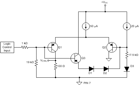 Figure 89. Logic Control Internal Schematic
The Q2 branch of the differential pair sets up a switch threshold approximately 1 V greater than the voltage applied to pin 7 (GND). If the control input is floating or < 0.7 V, the differential-pair tail current diverts to the 100-Ω detector load, and results in an output voltage (VCTRL, shown in Figure 89) that activates the desired mode. The floated pin default voltage is the PNP base current into the 19-kΩ resistor. As the control pin voltage rises above 1.3 V, the differential-pair current is completely diverted away from the 100 Ω side, thus switching states.
This unique design allows the logic control inputs to be connected to a single-supply as high as 15.9 V, in order to hold the inputs permanently high, while still accepting a low ground-referenced logic swing for single-supply operation. The NPN transistor (Q3) and two diodes (D1 and D2) act as a clamp to prevent large voltages from appearing across the differential stage.
When the OPS is disabled, both input paths to the OPS are also opened up regardless of the state of PATHSEL (pin 4).
9.4 Device Functional Modes
Any combination of the three internal blocks can be used separately, or in various combinations. The following sections describe the various functional modes of the THS3217.
9.4.1 Full-Signal Path Mode
The full-signal path from the D2S to the OPS is available in various options. Three options are described in the following subsections.
9.4.1.1 Internal Connection With Fixed Common-Mode Output Voltage
The most basic operation is to ground the VREF pin, and use the internal connection from the D2S to the OPS to provide a differential to single-ended, high-power driver. Figure 90 shows the characterization circuit used for the combined performance specifications.
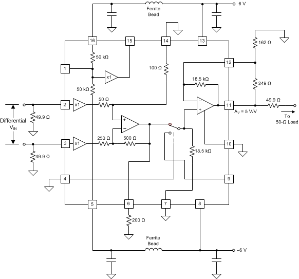 Figure 90. Differential to Single-Ended, Gain of 5-V/V Configuration
This configuration shows the test circuit used to generate Figure 1. Some of the key features in this basic configuration include:
- The power supplies are brought into the OPS first, then back to the input stage through a π-filter comprised of a ferrite bead and local decoupling caps on –VCC2 and +VCC2, pins 5 and 16, respectively (see the Power Supply Recommendations section for more information).
- The two logic lines are grounded. This logic configuration (with pin 7 grounded) selects the internal path from the D2S to OPS, and enables the OPS.
- The external I/O pins of the midscale buffer are left floating.
- The VREF pin is grounded, thus setting the D2S output common-mode voltage at VO1 (pin 6) to ground.
- The D2S external output is loaded with a 200-Ω resistor to ground. Lighter loading on the VO1 pin (versus the 100 Ω used to characterize the D2S only) results in increased frequency response peaking. Heavier loading degrades the D2S distortion performance.
- The external OPS input at pin 9 is left floating. However, it is internally tied to ground by the internal 18.5-kΩ resistor.
- The feedback resistor in the OPS is set to the parallel combination of the external 249-Ω resistor and the internal 18.5-kΩ resistor. This 245.7-Ω total RF with the 162-Ω RG resistor gives a gain of approximately 2.5 V/V (7.98 dB) in the OPS stage
- The input D2S gives a gain of 2 V/V (6 dB), and along with the 2.5 V/V (7.98 dB) from the OPS, gives an overall gain of 5 V/V (13.98 dB) with > 700 MHz of SSBW (see Figure 1).
9.4.1.2 Internal Connection With Adjustable Common-Mode Output Voltage
The simplest modification to this starting configuration is using the midscale buffer to drive the VREF pin with either a dc or ac source into VMID_IN (pin 1), shown in Figure 91.
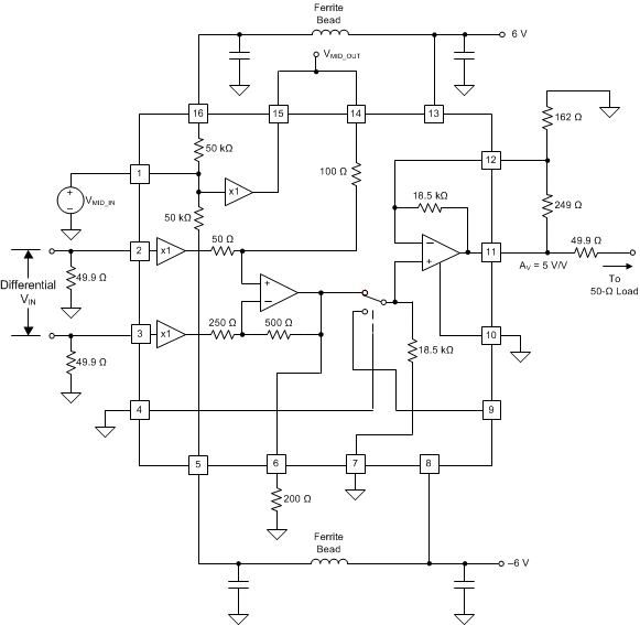 Figure 91. Differential to Single-Ended, Gain of 5-V/V Configuration With VREF Driven by the Midscale Buffer
The VREF input can be used to offset the output of the D2S that will then be amplified by the OPS. The total dc offset at the output of the OPS can also be corrected by adjusting the voltage at VMID_IN (pin 1). The on-chip midscale buffer can be used as a low-impedance source to drive the correction voltage to the VREF pin. A wideband small-signal source can also be summed into this path with a gain of 1 V/V to the D2S output pin. Figure 49 shows the midscale buffer to have an extremely flat response through 100 MHz for < 100-mVPPswings, while 1 VPP can be supported through 80 MHz with a flat response.
From this point on, the diagrams are simplified to not show the power-supply elements. However, the supplies are required by any application, as described in the Application and Implementation section.
9.4.1.3 External Connection
In the configuration shown in Figure 92, the bias to PATHSEL (pin 4) is changed in order to select the external input of the OPS. The external D2S output drives a low insertion loss, third-order Bessel filter. The filter in this example is designed with a low frequency insertion loss of 1.2 dB and f–3dB = 140 MHz, and results in an additional insertion loss of 1 dB at 100 MHz. The OPS gain is slightly increased to recover the filter loss, in order to give an input to output gain of 5 V/V. Using an interstage filter between the D2S and the OPS improves the step response by reducing the overshoot.
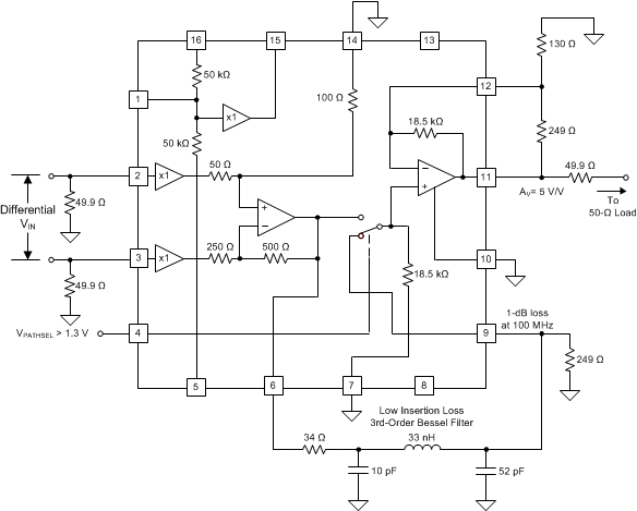 Figure 92. External Path Configuration With Interstage Low-Pass Filter
9.4.2 Dual-Output Mode
The D2S stage can also be used to directly drive a doubly-terminated line, as shown in Figure 93. In addition, the OPS amplifies the internal D2S output by 5 V/V. The internal path to the OPS is selected with PATHSEL (pin 4) at ground, and the OPS gain is increased to 5 V/V. A 2-VPP output at VO1 produces a 10-VPP output at VOUT (pin 11). This 10-VPP swing requires higher supply operation to provide sufficient headroom in the OPS output stage in order to preserve signal integrity. A power supply of ±7.5 V provides adequate headroom.
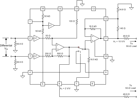 Figure 93. Dual-Output Mode
A simple modification to the circuit in Figure 93 is to disable the OPS, and switch to the external input path by taking both logic lines (pin 4 and pin 10) high. The D2S output at VO1 is then used either directly or through a filter to an even higher power driver like the ±15-V THS3091.
9.4.3 Differential I/O Voltage Mode
Having two amplifiers available also allows a simple differential I/O implementation with independent output common-mode control, as shown in Figure 94. In this configuration, the D2S provides one side of the differential output, while simultaneously driving the OPS configured in an inverting gain of –1 V/V to provide the differential output on the other side. The output at VMID_OUT biases the external noninverting input, VIN+ (pin 9). This circuit configuration places the differential input to the output filter at a common-mode voltage, VMID_OUT.
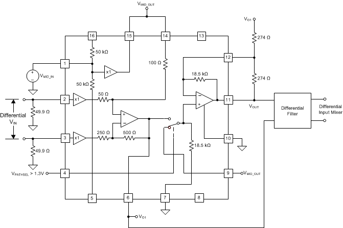 Figure 94. Differential I/O Configuration With Independent Output Common-Mode Voltage Control