ZHCSBP7C October 2013 – December 2018 TPS24750 , TPS24751
UNLESS OTHERWISE NOTED, this document contains PRODUCTION DATA.
- 1 特性
- 2 应用
- 3 说明
- 4 修订历史记录
- 5 Device Comparison Table
- 6 Pin Configuration and Functions
- 7 Specifications
- 8 Parameter Measurement Information
-
9 Detailed Descriptions
- 9.1 Overview
- 9.2 Functional Block Diagram
- 9.3 Feature Description
- 9.4 Device Functional Modes
-
10Application and Implementation
- 10.1 Application Information
- 10.2
Typical Application
- 10.2.1 Design Requirements
- 10.2.2
Detailed Design Procedure
- 10.2.2.1
Power-Limited Start-Up
- 10.2.2.1.1 STEP 1. Choose RSENSE, RSET, and RIMON
- 10.2.2.1.2 STEP 2. Choose Power-Limit Value, PLIM, and RPROG
- 10.2.2.1.3 STEP 3. Choose Output Voltage Rising Time, tON, and Timing Capacitor CT
- 10.2.2.1.4 STEP 4. Calculate the Retry-Mode Duty Ratio
- 10.2.2.1.5 STEP 5. Select R1, R2, and R3 for UV and OV
- 10.2.2.1.6 STEP 6. Choose R4, R5, and C1
- 10.2.2.2 Alternative Design Example: Gate Capacitor (dv/dt) Control in Inrush Mode
- 10.2.2.3 Additional Design Considerations
- 10.2.2.1
Power-Limited Start-Up
- 10.2.3 Application Curves
- 10.3 System Examples
- 11Power Supply Recommendations
- 12Layout
- 13器件和文档支持
- 14机械、封装和可订购信息
9.4.1 Board Plug-In
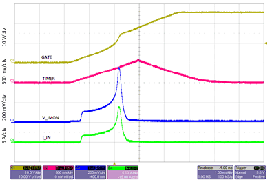
Figure 31 and Figure 32 illustrate the inrush current that flows when a hot swap board under the control of the TPS2475x is plugged into a system bus. Only the bypass capacitor charge current and small bias currents are evident when a board is first plugged in. The TPS2475x is held inactive for a short period while internal voltages stabilize. In this short period, GATE, PROG, and TIMER are held low and PGb, and FLTb, are held open-drain. When the voltage on the internal VCC rail exceeds approximately 1.5 V, the power-on reset (POR) circuit initializes the TPS2475x and a start-up cycle is ready to take place.
GATE, PROG, TIMER, PGb, and FLTb are released after the internal voltages have stabilized and the external EN (enable) thresholds have been exceeded. The part begins sourcing current from the GATE pin to turnon internal FET. The TPS2475x monitors both the drain-to-source voltage across internal MOSFET and the drain current passing through it. Based on these measurements, the TPS2475x limits the drain current by controlling the gate voltage so that the power dissipation of the internal FET does not exceed the power limit programmed by the user. The current increases as the voltage across the FET decreases until finally the current reaches the current limit ILIM.
 Figure 31. Inrush Mode at Hot-Swap Circuit Insertion