ZHCSAF5A OCTOBER 2012 – September 2016 TPS51716
PRODUCTION DATA.
- 1 特性
- 2 应用
- 3 说明
- 4 修订历史记录
- 5 Pin Configuration and Functions
- 6 Specifications
-
7 Detailed Description
- 7.1 Overview
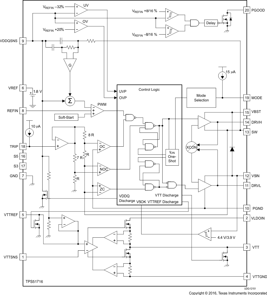
- 7.2 Functional Block Diagram
- 7.3
Feature Description
- 7.3.1 VDDQ Switch Mode Power Supply Control
- 7.3.2 VREF and REFIN, VDDQ Output Voltage
- 7.3.3 Soft-Start and Powergood
- 7.3.4 Power State Control
- 7.3.5 VDDQ Overvoltage and Undervoltage Protection
- 7.3.6 VDDQ Out-of-Bound Operation
- 7.3.7 VDDQ Overcurrent Protection
- 7.3.8 VTT and VTTREF
- 7.3.9 VTT Overcurrent Protection
- 7.3.10 V5IN Undervoltage Lockout (UVLO) Protection
- 7.3.11 Thermal Shutdown
- 7.4 Device Functional Modes
- 8 Application and Implementation
- 9 Power Supply Recommendations
- 10Layout
- 11器件和文档支持
- 12机械、封装和可订购信息
7 Detailed Description
7.1 Overview
The TPS51716 provides a complete power supply for DDR2, DDR3, DDR3L, LPDDR3, and DDR4 memory systems in the lowest total cost and minimum space. It integrates a synchronous buck regulator controller (VDDQ) with a 2-A sink/source tracking LDO (VTT) and buffered low noise reference (VTTREF). The TPS51716 employs D-CAP2 mode coupled with 500 kHz or 670 kHz operating frequencies that supports ceramic output capacitors without an external compensation circuit. The VTTREF tracks VDDQ/2 with excellent 0.8% accuracy. The VTT, which provides 2-A sink/source peak current capabilities, requires only 10-μF of ceramic capacitance. In addition, the device features a dedicated LDO supply input.
7.2 Functional Block Diagram

7.3 Feature Description
7.3.1 VDDQ Switch Mode Power Supply Control
The TPS51716 supports D-CAP2 mode, which does not require complex external compensation networks and are suitable for designs with small external components counts. The D-CAP2 mode is dedicated for a configuration with very low ESR output capacitors such as multi-layer ceramic capacitors (MLCC). An adaptive on-time control scheme is used to achieve pseudo-constant frequency. The TPS51716 adjusts the on-time (tON ) to be inversely proportional to the input voltage (VIN) and proportional to the output voltage (VVDDQ). This produces a switching frequency that is approximately constant over the variation of input voltage at the steady state condition.
7.3.2 VREF and REFIN, VDDQ Output Voltage
The part provides a 1.8-V, ±0.8% accurate, voltage reference from VREF. This output has a 300-μA (max) current capability to drive the REFIN input voltage through a voltage divider circuit. A capacitor with a value of 0.1-μF or larger should be attached close to the VREF terminal.
The VDDQ switch-mode power supply (SMPS) output voltage is defined by REFIN voltage, within the range between 0.7 V and 1.8 V, programmed by the resister-divider connected between VREF and GND. (See External Components Selection section.) A few nano farads of capacitance from REFIN to GND is recommended for stable operation.
7.3.3 Soft-Start and Powergood
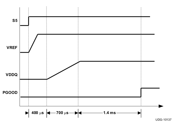
Provide a voltage supply to VIN and V5IN before asserting S5 to high. TPS51716 provides integrated VDDQ soft-start functions to suppress in-rush current at start-up. The soft-start is achieved by controlling internal reference voltage ramping up. Figure 22 shows the start-up waveforms. The switching regulator waits for 400μs after S5 assertion. The MODE pin voltage is read in this period. A typical VDDQ ramp up duration is 700μs.
TPS51716 has a powergood open-drain output that indicates the VDDQ voltage is within the target range. The target voltage window and transition delay times of the PGOOD comparator are ±8% (typ) and 1-ms delay for assertion (low to high), and ±16% (typ) and 330-ns delay for de-assertion (high to low) during running. The PGOOD start-up delay is 2.5 ms after S5 is asserted to high. Note that the time constant which is composed of the REFIN capacitor and a resistor divider needs to be short enough to reach the target value before PGOOD comparator enabled.
 Figure 22. Typical Start-Up Waveforms
7.3.4 Power State Control
The TPS51716 has two input pins, S3 and S5, to provide simple control scheme of power state. All of VDDQ, VTTREF and VTT are turned on at S0 state (S3=S5=high). In S3 state (S3=low, S5=high), VDDQ and VTTREF voltages are kept on while VTT is turned off and left at high impedance state (high-Z). The VTT output floats and does not sink or source current in this state. In S4/S5 states (S3=S5=low), all of the three outputs are turned off and discharged to GND according to the discharge mode selected by MODE pin. Each state code represents as follow; S0 = full ON, S3 = suspend to RAM (STR), S4 = suspend to disk (STD), S5 = soft OFF. (See Table 1.)
Table 1. S3/S5 Power State Control
| STATE | S3 | S5 | VREF | VDDQ | VTTREF | VTT |
|---|---|---|---|---|---|---|
| S0 | HI | HI | ON | ON | ON | ON |
| S3 | LO | HI | ON | ON | ON | OFF (High-Z) |
| S4/S5 | LO | LO | OFF | OFF (Discharge) | OFF (Discharge) | OFF (Discharge) |
7.3.5 VDDQ Overvoltage and Undervoltage Protection
The TPS51716 sets the overvoltage protection (OVP) when VDDQSNS voltage reaches a level 20% (typ) higher than the REFIN voltage. When an OV event is detected, the controller changes the output target voltage to 0 V. This usually turns off DRVH and forces DRVL to be on. When the inductor current begins to flow through the low-side MOSFET and reaches the negative OCL, DRVL is turned off and DRVH is turned on, for a minimum on-time.
After the minimum on-time expires, DRVH is turned off and DRVL is turned on again. This action minimizes the output node undershoot due to LC resonance. When the VDDQSNS reaches 0 V, the driver output is latched as DRVH off, DRVL on. VTTREF and VTT are turned off and discharged using the non-tracking discharge MOSFETs regardless of the tracking mode.
The undervoltage protection (UVP) latch is set when the VDDQSNS voltage remains lower than 68% (typ) of the REFIN voltage for 1 ms or longer. In this fault condition, the controller latches DRVH low and DRVL low and discharges the VDDQ, VTT and VTTREF outputs. UVP detection function is enabled after 1.2 ms of SMPS operation to ensure startup.
To release the OVP and UVP latches, toggle S5 or adjust the V5IN voltage down and up beyond the undervoltage lockout threshold.
7.3.6 VDDQ Out-of-Bound Operation
When the output voltage rises to 8% above the target value, the out-of-bound operation starts. During the out-of-bound condition, the controller operates in forced PWM-only mode. Turning on the low-side MOSFET beyond the zero inductor current quickly discharges the output capacitor. During this operation, the cycle-by-cycle negative overcurrent limit is also valid. Once the output voltage returns to within regulation range, the controller resumes to auto-skip mode.
7.3.7 VDDQ Overcurrent Protection
The VDDQ SMPS has cycle-by-cycle overcurrent limiting protection. The inductor current is monitored during the off-state using the low-side MOSFET RDS(on), and the controller maintains the off-state when the inductor current is larger than the overcurrent trip level. The current monitor circuit inputs are PGND and SW pins so that those should be properly connected to the source and drain terminals of low-side MOSFET. The overcurrent trip level, VOCTRIP, is determined by Equation 1, where RTRIP is the value of the resistor connected between the TRIP pin and GND, and ITRIP is the current sourced from the TRIP pin. ITRIP is 10 μA typically at room temperature, and has 4700ppm/°C temperature coefficient to compensate the temperature dependency of the low-side MOSFET RDS(on).

Because the comparison is done during the off-state, VOCTRIP sets the valley level of the inductor current. The load current OCL level, IOCL, can be calculated by considering the inductor ripple current as shown in Equation 2.

where
- IIND(ripple) is inductor ripple current
In an overcurrent condition, the current to the load exceeds the current to the output capacitor, thus the output voltage tends to fall down. Eventually, it crosses the undervoltage protection threshold and shuts down.
7.3.8 VTT and VTTREF
TPS51716 integrates two high performance, low-dropout linear regulators, VTT and VTTREF, to provide complete DDR2, DDR3, DDR3L, LPDDR3, and DDR4 power solutions. The VTTREF has a 10-mA sink/source current capability, and tracks ½ of VDDQSNS with ±1% accuracy using an on-chip ½ divider. A 0.22-μF (or larger) ceramic capacitor must be connected close to the VTTREF terminal to ensure stable operation. The VTT responds quickly to track VTTREF within ±40 mV at all conditions, and the current capability is 2 A for both sink and source. A 10-μF (or larger) ceramic capacitor(s) need to be connected close to the VTT terminal for stable operation. To achieve tight regulation with minimum effect of wiring resistance, a remote sensing terminal, VTTSNS, should be connected to the positive node of VTT output capacitor(s) as a separate trace from the high-current line to the VTT pin. (Refer to the Layout Guidelines section for details.)
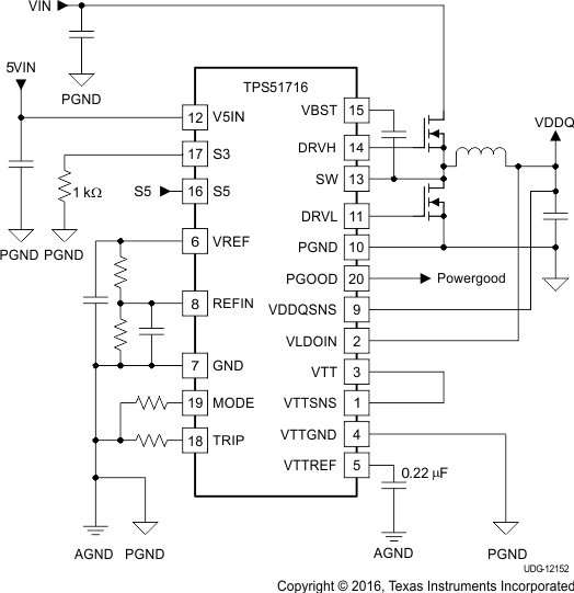
When VTT is not required in the design, the following treatment is strongly recommended.
- Connect VLDOIN to VDDQ.
- Tie VTTSNS to VTT, and remove capacitors from VTT to float.
- Connect VTTGND to GND.
- Select MODE2, 3, 4, or 5 shown in Table 2 (Select Non-tracking discharge mode).
- Maintain a 0.22-µF capacitor connected at VTTREF.
- Pull down S3 to GND with 1-kΩ resistance.
 Figure 23. Application Circuit When VTT is not Required
7.3.9 VTT Overcurrent Protection
The LDO has an internally fixed constant overcurrent limiting of 3-A (typ) for both sink and source operation.
7.3.10 V5IN Undervoltage Lockout (UVLO) Protection
The TPS51716 has a 5-V supply UVLO protection threshold. When the V5IN voltage is lower than UVLO threshold voltage, typically 3.9 V, VDDQ, VTT, and VTTREF are shut off. This is a non-latch protection.
7.3.11 Thermal Shutdown
The TPS51716 includes an internal temperature monitor. If the temperature exceeds the threshold value, 140°C (typ), VDDQ, VTT, and VTTREF are shut off. The state of VDDQ is open, and that of VTT and VTTREF are high impedance (high-Z) at thermal shutdown. The discharge functions of all outputs are disabled. This is a non-latch protection and the operation is restarted with soft-start sequence when the device temperature is reduced by 10°C (typ).
7.4 Device Functional Modes
7.4.1 MODE Pin Configuration
The TPS51716 reads the MODE pin voltage when the S5 signal is raised high and stores the status in a register. A 15-μA current is sourced from the MODE pin during this time to read the voltage across the resistor connected between the pin and GND. Table 2 shows resistor values, corresponding control mode, switching frequency and discharge mode configurations.
Table 2. MODE Selection
| MODE NO. | RESISTANCE BETWEEN MODE AND GND (kΩ) |
CONTROL MODE |
SWITCHING FREQUENCY (kHz) |
DISCHARGE MODE |
|---|---|---|---|---|
| 3 | 33 | D-CAP2 | 500 | Non-Tracking |
| 2 | 22 | 670 | ||
| 1 | 12 | 670 | Tracking | |
| 0 | 1 | 500 |
7.4.2 Discharge Control
In S4/S5 state, VDDQ, VTT, and VTTREF outputs are discharged based on the respective discharge mode selected above. The tracking discharge mode discharges VDDQ output through the internal VTT regulator transistors enabling quick 13 ms discharge operation. The VTT output maintains tracking of the VTTREF voltage in this mode. (Please refer to Figure 28) After 4 ms of tracking discharge operation, the mode changes to non-tracking discharge. The VDDQ output must be connected to the VLDOIN pin in this mode. The non-tracking mode discharges the VDDQ and VTT pins using internal MOSFETs that are connected to corresponding output terminals. The non-tracking discharge is slow compared with the tracking discharge due to the lower current capability of these MOSFETs. Refer to Figure 29.
7.4.3 D-CAP2 Mode Operation
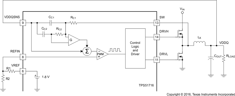
Figure 24 shows simplified model of D-CAP2 architecture.
 Figure 24. Simplified Modulator Using D-CAP2 Mode
The D-CAP2 mode in the TPS51716 includes an internal feedback network enabling the use of very low ESR output capacitor(s) such as multi-layer ceramic capacitors. The role of the internal network is to sense the ripple component of the inductor current information and combine it with voltage feedback signal. Using RC1 = RC2 ≡ RC and CC1 = CC2 ≡ CC, 0-dB frequency of the D-CAP2 mode is given by Equation 3. It is recommended that the 0-dB frequency (f0) be lower than 1/3 of the switching frequency to secure the proper phase margin.

where
- G is gain of the amplifier which amplifies the ripple current information generated by the compensation circuit
The typical G value is 0.25, and typical RCCC time constant values for 500 kHz and 670 kHz operation are 23 µs and 14.6 µs, respectively.
For example, when fSW=500 kHz and LX=1 µH, COUT should be larger than 88 µF.
When selecting the capacitor, pay attention to its characteristics. For MLCC use X5R or better dielectric and consider the derating of the capacitance by both DC bias and AC bias. When derating by DC bias and AC bias are 80% and 50%, respectively, the effective derating is 40% because 0.8 x 0.5 = 0.4. The capacitance of specialty polymer capacitors may change depending on the operating frequency. Consult capacitor manufacturers for specific characteristics.
7.4.4 Light-Load Operation
In auto-skip mode, the TPS51716 SMPS control logic automatically reduces its switching frequency to improve light-load efficiency. To achieve this intelligence, a zero cross detection comparator is used to prevent negative inductor current by turning off the low-side MOSFET. Equation 4 shows the boundary load condition of this skip mode and continuous conduction operation.
