SBVS054J November 2004 – April 2015 TPS730
PRODUCTION DATA.
- 1 Features
- 2 Applications
- 3 Description
- 4 Revision History
- 5 Pin Configuration and Functions
- 6 Specifications
- 7 Detailed Description
- 8 Application and Implementation
- 9 Power Supply Recommendations
- 10Layout
- 11Device and Documentation Support
- 12Mechanical, Packaging, and Orderable Information
8 Application and Implementation
NOTE
Information in the following applications sections is not part of the TI component specification, and TI does not warrant its accuracy or completeness. TI’s customers are responsible for determining suitability of components for their purposes. Customers should validate and test their design implementation to confirm system functionality.
8.1 Application Information
The TPS730 family of low-dropout (LDO) regulators has been optimized for use in noise-sensitive battery-operated equipment. The device features extremely low dropout voltages, high PSRR, ultra-low output noise, low quiescent current (170 μA typically), and enable-input to reduce supply currents to less than 1 μA when the regulator is turned off.
8.1.1 Adjustable Operation
The output voltage of the TPS73001 adjustable regulator is programmed using an external resistor divider as shown in Figure 17. The output voltage is calculated using Equation 1:

where
- VREF = 1.225 V typical (the internal reference voltage)
Resistors R1 and R2 should be chosen for approximately 50-μA divider current. Lower value resistors can be used for improved noise performance, but the solution consumes more power. Higher resistors values can cause accuracy issues and other problems. The recommended design procedure is to choose R2 = 30.1 kΩ to set the divider current at 50 μA, C1 = 15 pF for stability, and then calculate R1 using Equation 2:

To improve the stability of the adjustable version, TI suggests placing a small compensation capacitor between OUT and FB. For output voltages < 1.8 V, the value of this capacitor should be 100 pF. For output voltages > 1.8 V, use Equation 3 to calculate the approximate value of this capacitor.

Figure 17 shows the suggested value of this capacitor for several resistor ratios. If this capacitor is not used (such as in a unity-gain configuration) or if an output voltage < 1.8 V is chosen, then the minimum recommended output capacitor is 4.7 μF instead of 2.2 μF.
 Figure 17. TPS73001 Adjustable LDO Regulator Programming
8.1.2 Capacitor Recommendations
Low equivalent series resistance (ESR) capacitors should be used for the input, output, noise reduction, and bypass capacitors. Ceramic capacitors with X7R and X5R dielectrics are preferred. These dielectrics offer more stable characteristics. Ceramic X7R capacitors offer improved overtemperature performance, while ceramic X5R capacitors are more cost-effective and are available in higher values.
8.1.3 Input and Output Capacitor Requirements
A 0.1-μF or larger ceramic input bypass capacitor, connected between IN and GND and located close to the TPS730, is required for stability and improves transient response, noise rejection, and ripple rejection. A higher-value input capacitor may be necessary if large, fast-rise-time load transients are anticipated or the device is located several inches from the power source.
Like most low-dropout regulators, the TPS730 requires an output capacitor connected between OUT and GND to stabilize the internal control loop. The minimum recommended capacitance is 2.2 μF. Any 2.2-μF or larger ceramic capacitor is suitable, provided the capacitance does not vary significantly over temperature. If load current is not expected to exceed 100 mA, a 1-μF ceramic capacitor can be used. If a feed-forward capacitor is not used (such as in a unity-gain configuration) or if an output voltage less than 1.8 V is chosen, then the minimum recommended output capacitor is 4.7 μF instead of 2.2 μF. Table 2 lists the recommended output capacitor sizes for several common configurations.
Table 2. Output Capacitor Sizing
| CONDITION | COUT (µF) |
|---|---|
| VOUT < 1.8 V or CFF = 0 nF | 4.7 |
| VOUT > 1.8 V, IOUT > 100 mA | 2.2 |
| VOUT > 1.8 V, IOUT < 100 mA | 1 |
8.1.4 Noise Reduction and Feed-Forward Capacitor Requirements
The internal voltage reference is a key source of noise in an LDO regulator. The TPS730 has an NR pin which is connected to the voltage reference through a 250-kΩ internal resistor. The 250-kΩ internal resistor, in conjunction with an external bypass capacitor connected to the NR pin, creates a low-pass filter to reduce the voltage reference noise and, therefore, the noise at the regulator output. In order for the regulator to operate properly, the current flow out of the NR pin must be at a minimum, because any leakage current creates an IR drop across the internal resistor thus creating an output error. Therefore, the bypass capacitor must have minimal leakage current. The bypass capacitor should be no more than 0.1 μF to ensure that it is fully charged during the quick-start time provided by the internal switch shown in the Functional Block Diagram section.
As an example, the TPS73018 exhibits only 33 μVRMS of output voltage noise using a 0.01-μF ceramic bypass capacitor and a 2.2-μF ceramic output capacitor. Note that the output starts up slower as the bypass capacitance increases due to the RC time constant at the NR pin that is created by the internal 250-kΩ resistor and external capacitor.
A feed-forward capacitor is recommended to improve the stability of the device. If R2 = 30.1 kΩ, set C1 to 15 pF for optimal performance. For voltages less than 1.8 V, the value of this capacitor should be 100 pF. For voltages greater than 1.8 V, the approximate value of this capacitor can be calculated as shown in Equation 3.
8.1.5 Reverse Current Operation
The TPS730 PMOS-pass transistor has a built-in back diode that conducts reverse current when the input voltage drops below the output voltage (for example, during power-down). Current is conducted from the output to the input and is not internally limited. If extended reverse voltage operation is anticipated, external limiting might be appropriate. If extended reverse voltage operation in anticipated, external limiting to 5% of the rated output current is recommended.
8.2 Typical Application
A typical application circuit is shown in Figure 18.
 Figure 18. Typical Application Circuit
8.2.1 Design Requirements
Table 3 lists the design requirements.
Table 3. Design Parameters
| PARAMETER | DESIGN REQUIREMENT |
|---|---|
| Input voltage | 4.2 V to 3 V (Lithium Ion battery) |
| Output voltage | 1.8 V, ±1% |
| DC output current | 10 mA |
| Peak output current | 75 mA |
| Maximum ambient temperature | 65°C |
8.2.2 Detailed Design Procedure
Pick the desired output voltage option. An input capacitor of 0.1 µF is used as the battery is connected to the input through a via and a short 10-mil (0.01-in) trace. An output capacitor of 10 µF is used to provide optimal response time for the load transient. Verify that the maximum junction temperature is not exceed by referring to Figure 24.
8.2.3 Application Curves
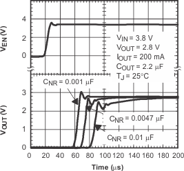
 Figure 19. TPS73028 Output Voltage, Enable Voltage vs Time (Start-Up)
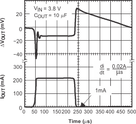
 Figure 21. TPS73028 Load Transient Response
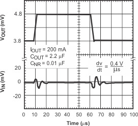
 Figure 20. TPS73028 Line Transient Response
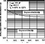
 Figure 22. Typical Regions of Stability Equivalent Series Resistance (ESR) vs Output Current
8.3 Do's and Don'ts
Do place at least one, low-ESR, 2.2-μF capacitor as close as possible between the OUT pin of the regulator and the GND pin.
Do place at least one, low-ESR, 0.1-μF capacitor as close as possible between the IN pin of the regulator and the GND pin.
Do provide adequate thermal paths away from the device.
Do not place the input or output capacitor more than 10 mm away from the regulator.
Do not exceed the absolute maximum ratings.
Do not float the Enable (EN) pin.
Do not resistively or inductively load the NR pin.
Do not let the output voltage get more than 0.3 V above the input voltage.