ZHCSGL0A April 2017 – August 2017 TPS7H1101A-SP
PRODUCTION DATA.
7 Detailed Description
7.1 Overview
The TPS7H1101A-SP is 3-A, 1.5-V to 7-V LDO linear regulator that uses PMOS pass element configuration.
It uses TI’s proprietary process to achieve low noise, high PSRR combined with high-thermal performance in a 16-pin ceramic flatpack package (HKR).
A number of features are incorporated in the design to provide high reliability and system flexibility. Current foldback, current limit, and thermal protection are incorporated in the design to make it viable for harsh environments.
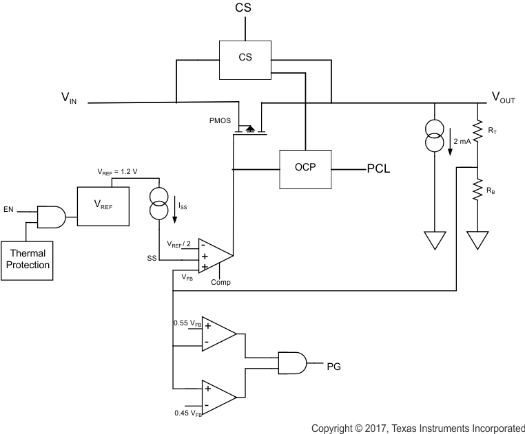
The device also has a current sense monitoring feature. A resistor connected from the current sense (CS) terminal to VIN indicates voltage proportional to the output current. When CS is held high, foldback current limit is enabled. Shorting CS low disables the foldback current limit.
A resistor connected from the programmable current limit (PCL) terminal to ground sets the overcurrent limit activation point. When overcurrent limit activation point is reached, it results in LDO going into current foldback mode. Output current is reduced to approximately 50% of the current limit set point. The PCL section provides a detailed description of this feature.
TPS7H1101A-SP incorporates thermal protection, which disables the output when the junction temperature rises approximately 185°C, allowing the device to cool. Cycling limits the dissipation of the regulator, protecting it from damage as a result of overheating.
A resistor connected from the CS terminal to VIN indicates voltage proportional to the output load current.
To provide system flexibility for demanding current needs, the LDO can be configured in parallel operation as indicated in Figure 20. The Current Sharing section provides detailed parallel operation information.
An enable feature is incorporated in the design allowing the user to enable or disable the LDO. Power Good, an open-drain connection, indicates the status of the output voltage. These provide the customers system flexibility in monitoring and controlling the LDO operation.
7.2 Functional Block Diagram

7.3 Feature Description
7.3.1 Soft Start
Connecting a capacitor from the SS terminal to GND (CSS) slows down the output voltage ramp rate. The soft-start capacitor charges up to 1.2 V.

where
- tss = soft-start time
- Iss = 2.5 µA
- VFB = VREF / 2 = 0.605 V
7.3.2 Power Good (PG)
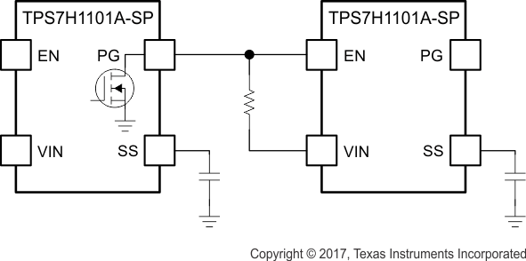
Power Good terminal (9) is an open-drain connection and can be used to sequence multiple LDOs. Figure 8 shows typical connection. The PG terminal will be pulled low until the output voltage reaches 90% of its maximum level. At that point, the PG pin will be pulled up. Since the PG pin is open drain, it can be pulled up to any voltage as long as it does not exceed the absolute max of 7.5 V listed in the Electrical Characteristics table.
 Figure 8. Sequencing LDOs with Power Good
NOTE
For PSpice models, WEBENCH, and mini-POL reference design, see the Tools & Software tab.
- PSpice average model (stability – Bode plot)
- PSpice transient model (switching waveforms)
- WEBENCH design tool, www.ti.com/product/TPS7H1101A-SP/toolssoftware
7.4 Device Functional Modes
7.4.1 Enable/Disable
For VIN from 1.5 V to 7 V, TPS7H1101A-SP can be disabled by pulling the enable terminal to logic low at a minimum of 0.7 V. In all cases, the enable terminal should be connected to VIN.