ZHCSGC2I June   2017  – March 2024 UCC5310 , UCC5320 , UCC5350 , UCC5390

PRODUCTION DATA  

  1.   1
  2. 特性
  3. 应用
  4. 说明
  5. Device Comparison Table
  6. Pin Configuration and Function
  7. Specifications
    1. 6.1  Absolute Maximum Ratings
    2. 6.2  ESD Ratings
    3. 6.3  Recommended Operating Conditions
    4. 6.4  Thermal Information
    5. 6.5  Power Ratings
    6. 6.6  Insulation Specifications for D Package
    7. 6.7  Insulation Specifications for DWV Package
    8. 6.8  Safety-Related Certifications For D Package
    9. 6.9  Safety-Related Certifications For DWV Package
    10. 6.10 Safety Limiting Values
    11. 6.11 Electrical Characteristics
    12. 6.12 Switching Characteristics
    13. 6.13 Insulation Characteristics Curves
    14. 6.14 Typical Characteristics
  8. Parameter Measurement Information
    1. 7.1 Propagation Delay, Inverting, and Noninverting Configuration
      1. 7.1.1 CMTI Testing
  9. Detailed Description
    1. 8.1 Overview
    2. 8.2 Functional Block Diagram
    3. 8.3 Feature Description
      1. 8.3.1 Power Supply
      2. 8.3.2 Input Stage
      3. 8.3.3 Output Stage
      4. 8.3.4 Protection Features
        1. 8.3.4.1 Undervoltage Lockout (UVLO)
        2. 8.3.4.2 Active Pulldown
        3. 8.3.4.3 Short-Circuit Clamping
        4. 8.3.4.4 Active Miller Clamp (UCC53x0M)
    4. 8.4 Device Functional Modes
      1. 8.4.1 ESD Structure
  10. Application and Implementation
    1. 9.1 Application Information
    2. 9.2 Typical Application
      1. 9.2.1 Design Requirements
      2. 9.2.2 Detailed Design Procedure
        1. 9.2.2.1 Designing IN+ and IN– Input Filter
        2. 9.2.2.2 Gate-Driver Output Resistor
        3. 9.2.2.3 Estimate Gate-Driver Power Loss
        4. 9.2.2.4 Estimating Junction Temperature
      3. 9.2.3 Selecting VCC1 and VCC2 Capacitors
        1. 9.2.3.1 Selecting a VCC1 Capacitor
        2. 9.2.3.2 Selecting a VCC2 Capacitor
        3. 9.2.3.3 Application Circuits with Output Stage Negative Bias
      4. 9.2.4 Application Curve
  11. 10Power Supply Recommendations
  12. 11Layout
    1. 11.1 Layout Guidelines
    2. 11.2 Layout Example
    3. 11.3 PCB Material
  13. 12Device and Documentation Support
    1. 12.1 Device Support
      1. 12.1.1 第三方米6体育平台手机版_好二三四免责声明
    2. 12.2 Documentation Support
      1. 12.2.1 Related Documentation
    3. 12.3 Certifications
    4. 12.4 接收文档更新通知
    5. 12.5 支持资源
    6. 12.6 Trademarks
    7. 12.7 静电放电警告
    8. 12.8 术语表
  14. 13Revision History
  15. 14Mechanical, Packaging, and Orderable Information

封装选项

机械数据 (封装 | 引脚)
散热焊盘机械数据 (封装 | 引脚)
订购信息

Typical Application

The circuits in Figure 9-1, Figure 9-2, and Figure 9-3 show a typical application for driving IGBTs.
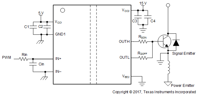
GUID-11CF1C5B-540C-4DA0-B47A-0F424B189572-low.gif Figure 9-1 Typical Application Circuit for UCC53x0S to Drive IGBT
GUID-E4FAD271-3E63-462B-A506-44CC132C66D6-low.gif Figure 9-2 Typical Application Circuit for UCC5310M and UCC5350M to Drive IGBT
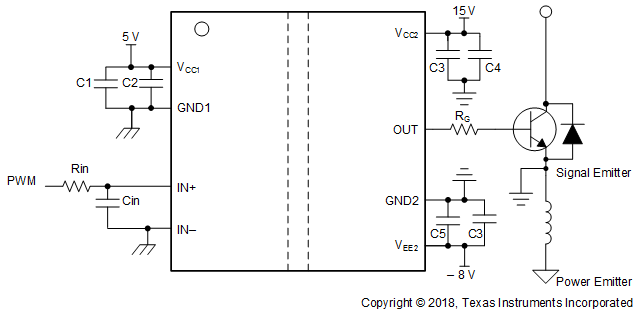
GUID-43214B9B-ABE7-4035-BAC5-998F825617CE-low.gif Figure 9-3 Typical Application Circuit for UCC5320E and UCC5390E to Drive IGBT