ZHCSMR1C october   2019  – september 2021 UCC5870-Q1

PRODUCTION DATA  

  1. 特性
  2. 应用
  3. 说明
  4. Revision History
  5. Pin Configuration and Functions
  6. Specifications
    1. 6.1  Absolute Maximum Ratings
    2. 6.2  ESD Ratings
    3. 6.3  Recommended Operating Conditions
    4. 6.4  Thermal Information
    5. 6.5  Power Ratings
    6. 6.6  Insulation Specifications
    7. 6.7  Electrical Characteristics
    8. 6.8  SPI Timing Requirements
    9. 6.9  Switching Characteristics
    10. 6.10 Typical Characteristics
  7. Detailed Description
    1. 7.1 Overview
    2. 7.2 Functional Block Diagram
    3. 7.3 Feature Description
      1. 7.3.1 Power Supplies
        1. 7.3.1.1 VCC1
        2. 7.3.1.2 VCC2
        3. 7.3.1.3 VEE2
        4. 7.3.1.4 VREG1
        5. 7.3.1.5 VREG2
        6. 7.3.1.6 VREF
        7. 7.3.1.7 Other Internal Rails
      2. 7.3.2 Driver Stage
      3. 7.3.3 Integrated ADC for Front-End Analog (FEA) Signal Processing
        1. 7.3.3.1 AI* Setup
        2. 7.3.3.2 ADC Setup and Sampling Modes
          1. 7.3.3.2.1 Center Sampling Mode
          2. 7.3.3.2.2 Edge Sampling Mode
          3. 7.3.3.2.3 Hybrid Mode
        3. 7.3.3.3 DOUT Functionality
      4. 7.3.4 Fault and Warning Classification
      5. 7.3.5 Diagnostic Features
        1. 7.3.5.1  Undervoltage Lockout (UVLO) and Overvoltage Lockout (OVLO)
          1. 7.3.5.1.1 Built-In Self Test (BIST)
            1. 7.3.5.1.1.1 Analog Built-In Self Test (ABIST)
            2. 7.3.5.1.1.2 Function BIST
            3. 7.3.5.1.1.3 Clock Monitor
              1. 7.3.5.1.1.3.1 Clock Monitor Built-In Self Test
        2. 7.3.5.2  CLAMP, OUTH, and OUTL Clamping Circuits
        3. 7.3.5.3  Active Miller Clamp
        4. 7.3.5.4  DESAT based Short Circuit Protection (DESAT)
        5. 7.3.5.5  Shunt Resistor based Overcurrent Protection (OCP) and Short Circuit Protection (SCP)
        6. 7.3.5.6  Temperature Monitoring and Protection for the Power Transistors
        7. 7.3.5.7  Active High Voltage Clamping (VCECLP)
        8. 7.3.5.8  Two-Level Turn-Off
        9. 7.3.5.9  Soft Turn-Off (STO)
        10. 7.3.5.10 Thermal Shutdown (TSD) and Temperature Warning (TWN) of Driver IC
        11. 7.3.5.11 Active Short Circuit Support (ASC)
        12. 7.3.5.12 Shoot-Through Protection (STP)
        13. 7.3.5.13 Gate Voltage Monitoring and Status Feedback
        14. 7.3.5.14 VGTH Monitor
        15. 7.3.5.15 Cyclic Redundancy Check (CRC)
          1. 7.3.5.15.1 Calculating CRC
        16. 7.3.5.16 Configuration Data CRC
        17. 7.3.5.17 SPI Transfer Write/Read CRC
          1. 7.3.5.17.1 SDI CRC Check
          2. 7.3.5.17.2 SDO CRC Check
        18. 7.3.5.18 TRIM CRC Check
    4. 7.4 Device Functional Modes
      1. 7.4.1 State 1: RESET
      2. 7.4.2 State 2: Configuration 1
      3. 7.4.3 State 3: Configuration 2
      4. 7.4.4 State 4: Active
    5. 7.5 Programming
      1. 7.5.1 SPI Communication
        1. 7.5.1.1 System Configuration of SPI Communication
          1. 7.5.1.1.1 Independent Slave Configuration
          2. 7.5.1.1.2 Daisy Chain Configuration
          3. 7.5.1.1.3 Address-based Configuration
        2. 7.5.1.2 SPI Data Frame
          1. 7.5.1.2.1 Writing a Register
          2. 7.5.1.2.2 Reading a Register
    6. 7.6 Register Maps
      1. 7.6.1 UCC5870 Registers
  8. Applications and Implementation
    1. 8.1 Application Information
      1. 8.1.1 Power Dissipation Considerations
      2. 8.1.2 Device Addressing
    2. 8.2 Typical Application Using Internal ADC Reference and Power FET Sense Current Monitoring
      1. 8.2.1 Design Requirements
      2. 8.2.2 Detailed Design Procedure
        1. 8.2.2.1 VCC1, VCC2, and VEE2 Bypass Capacitors
        2. 8.2.2.2 VREF, VREG1, and VREG2 Bypass Capacitors
        3. 8.2.2.3 Bootstrap Capacitor (VBST)
        4. 8.2.2.4 VCECLP Input
        5. 8.2.2.5 External CLAMP Output
        6. 8.2.2.6 AI* Inputs
        7. 8.2.2.7 OUTH/ OUTL Outputs
        8. 8.2.2.8 nFLT* Outputs
      3. 8.2.3 Application Curves
    3. 8.3 Typical Application Using DESAT Power FET Monitoring
      1. 8.3.1 Detailed Design Procedure
        1. 8.3.1.1 DESAT Input
      2. 8.3.2 Application Curves
  9. Power Supply Recommendations
    1. 9.1 VCC1 Power Supply
    2. 9.2 VCC2 Power Supply
    3. 9.3 VEE2 Power Supply
    4. 9.4 VREF Supply (Optional)
  10. 10Layout
    1. 10.1 Layout Guidelines
      1. 10.1.1 Component Placement
      2. 10.1.2 Grounding Considerations
      3. 10.1.3 High-Voltage Considerations
      4. 10.1.4 Thermal Considerations
    2. 10.2 Layout Example
  11. 11Device and Documentation Support
    1. 11.1 Documentation Support
      1. 11.1.1 Related Documentation
    2. 11.2 Receiving Notification of Documentation Updates
    3. 11.3 支持资源
    4. 11.4 Trademarks
    5. 11.5 静电放电警告
    6. 11.6 术语表
  12. 12Mechanical, Packaging, and Orderable Information

封装选项

机械数据 (封装 | 引脚)
散热焊盘机械数据 (封装 | 引脚)
订购信息

Active High Voltage Clamping (VCECLP)

The active high voltage clamping feature protects power transistors from over-voltage damage during switching transitions, while reducing the power dissipated in the external TVS clamp diodes protecting the power FET. During turn-off, the VCECLP input is monitored. Once the VCE of the FET increases to turn on the external TVS diode, the RC network on the VCECLP input is charged up. Once the VCECLP input reaches the clamp threshold (VCECLPTH), OUTL drive strength changes to the ISTO setting in order to slow down the turn off and reduce the overshoot. The high voltage clamping remains active for a predefined time tVCECLP_HLD. The OV condition is reported in STATUS3[VCEOV_FAULT] (STATUS3). The implementation and timing diagrams for the active high voltage clamping are presented in Figure 7-22 and Figure 7-23, respectively. The VCECLP feature is enabled/disabled using the CFG4[VCECLP_EN] bit (CFG4).
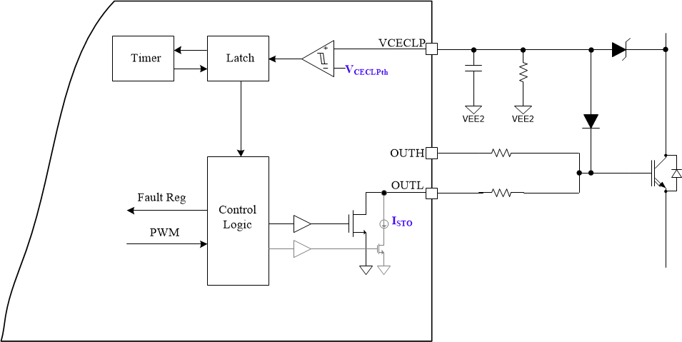
GUID-D36538B5-740E-4D77-8E2A-A50D4D0AE8C7-low.png Figure 7-22 Block diagram of implementation of active high voltage clamping function.
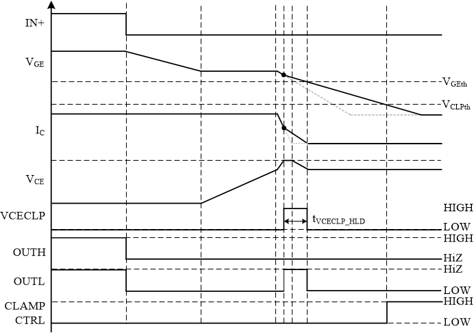
GUID-53A9D868-8373-4189-8055-5FC79CCE69E8-low.png Figure 7-23 Timing scheme of implementation of active high voltage clamping function.