ZHCSMR1C october 2019 – september 2021 UCC5870-Q1
PRODUCTION DATA
- 1 特性
- 2 应用
- 3 说明
- 4 Revision History
- 5 Pin Configuration and Functions
- 6 Specifications
-
7 Detailed Description
- 7.1 Overview
- 7.2 Functional Block Diagram
- 7.3
Feature Description
- 7.3.1 Power Supplies
- 7.3.2 Driver Stage
- 7.3.3 Integrated ADC for Front-End Analog (FEA) Signal Processing
- 7.3.4 Fault and Warning Classification
- 7.3.5
Diagnostic Features
- 7.3.5.1 Undervoltage Lockout (UVLO) and Overvoltage Lockout (OVLO)
- 7.3.5.2 CLAMP, OUTH, and OUTL Clamping Circuits
- 7.3.5.3 Active Miller Clamp
- 7.3.5.4 DESAT based Short Circuit Protection (DESAT)
- 7.3.5.5 Shunt Resistor based Overcurrent Protection (OCP) and Short Circuit Protection (SCP)
- 7.3.5.6 Temperature Monitoring and Protection for the Power Transistors
- 7.3.5.7 Active High Voltage Clamping (VCECLP)
- 7.3.5.8 Two-Level Turn-Off
- 7.3.5.9 Soft Turn-Off (STO)
- 7.3.5.10 Thermal Shutdown (TSD) and Temperature Warning (TWN) of Driver IC
- 7.3.5.11 Active Short Circuit Support (ASC)
- 7.3.5.12 Shoot-Through Protection (STP)
- 7.3.5.13 Gate Voltage Monitoring and Status Feedback
- 7.3.5.14 VGTH Monitor
- 7.3.5.15 Cyclic Redundancy Check (CRC)
- 7.3.5.16 Configuration Data CRC
- 7.3.5.17 SPI Transfer Write/Read CRC
- 7.3.5.18 TRIM CRC Check
- 7.4 Device Functional Modes
- 7.5 Programming
- 7.6 Register Maps
- 8 Applications and Implementation
- 9 Power Supply Recommendations
- 10Layout
- 11Device and Documentation Support
- 12Mechanical, Packaging, and Orderable Information
7.3.5.4 DESAT based Short Circuit Protection (DESAT)
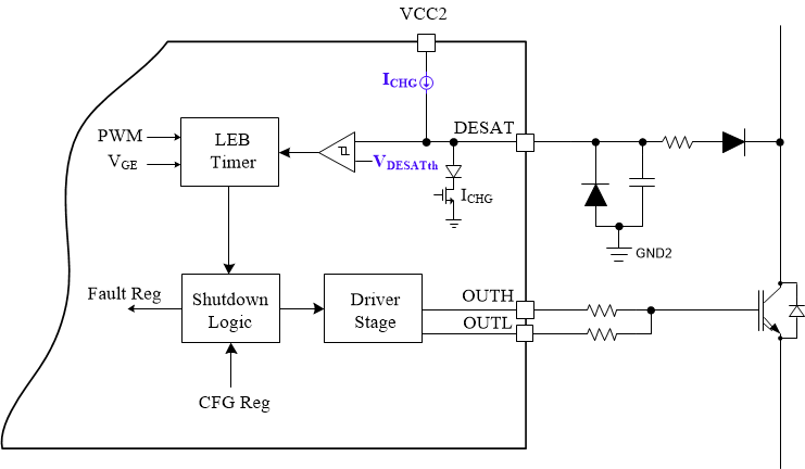
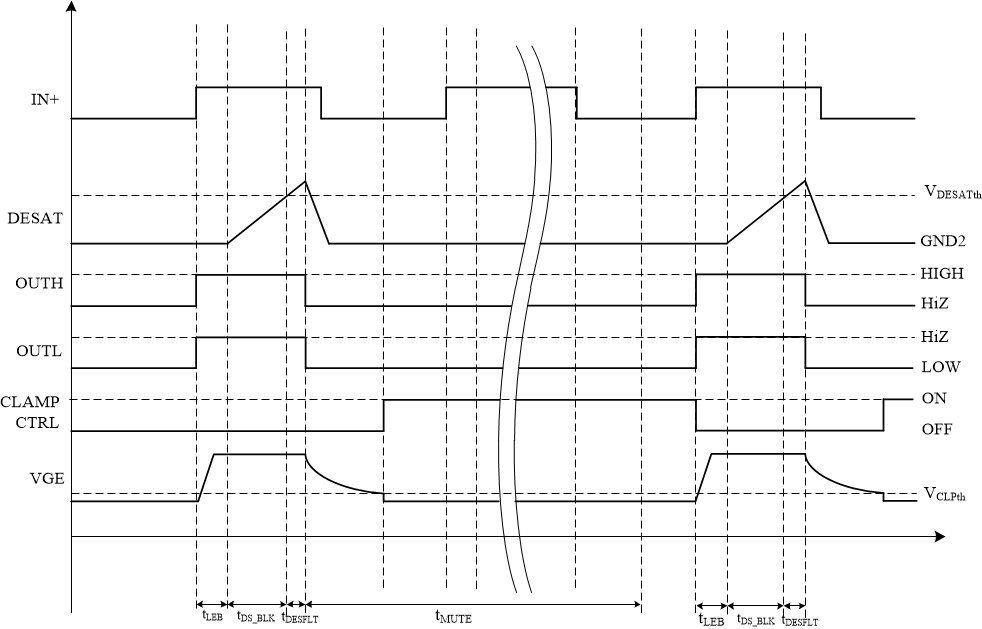
DESAT protection prevents the power transistor from damage in case of short circuit faults. The DESAT input monitors the VCEsat (IGBT)/VDSon (MOSFET) through an external resistor and diode network (R1, C1, D1 and D2 in Figure 7-16). The D1 diode protects the driver IC from high voltage when the power transistor is OFF. The resistor, R1, limits the negative voltage applied on the DESAT input during switching transitions. While the power FET is ON, an internal current source, ICHG, forward biases the DESAT diode and dumps into the collector/drain of the external power switch. Under normal conditions, the VCEsat/VDSon is less than a few volts, however, during short circuit faults the VCEsat/VDSon may rise up to the DC bus voltage when the power transistor operates in the linear region. In this situation, the D1 diode is reverse biased, so the internal current source charges the blanking capacitor (C1) Once the voltage on the DESAT input charges up to the selected threshold (VDESATth),the driver output is pulled into the safe state defined by the CFG10[FS_STATE_DESAT_SCP] bit (CFG10), the fault is indicated in the STATUS3[DESAT_FAULT] (STATUS3), and, if unmasked, the NFLT1 output pulls low. The turn-off of the driver output during a DESAT fault is selectable between normal, soft turn-off (STO), or two-level turnoff (2LTO) dictated by the CFG5[2LTOFF_STO_EN] bits (CFG5). See the Section 7.3.5.9and Section 7.3.5.8 for additional details on STO and 2LTO, respectively. The blanking capacitor is fully discharged at the falling edge of the PWM signal using the internal discharge current (IDCHG). In addition to the blanking time, DESAT is deglitched to prevent false triggering during transitions. The deglitch is selectable using the CFG4[DESAT_DEGLITCH] bit (CFG4).
The DESAT threshold is selectable using the CFG5[DESATTH] bits (CFG5), and the DESAT charging current (ICHG) is selectable, using the CFG5[DESAT_CHG_CURR] bits (CFG5), to control the blanking time (tDS_BLK). The discharge current is enabled/disabled using the CFG5[DESAT_DCHG_EN] bit (CFG5). The DESAT protection function is enabled or disabled using the CFG4[DESAT_EN] bit (CFG4). The implementation diagram and timing schemes of DESAT based short circuit protection are presented in Figure 7-16 and Figure 7-17 respectively. See the Section 8.3.1.1section for details on selecting the R1, C1, and D1 values.
 Figure 7-16 Block diagram of implementation of
DESAT protection function.
 Figure 7-17 Timing scheme of implementation of
DESAT protection function (safe state is LOW).