ZHCSMR1C october 2019 – september 2021 UCC5870-Q1
PRODUCTION DATA
- 1 特性
- 2 应用
- 3 说明
- 4 Revision History
- 5 Pin Configuration and Functions
- 6 Specifications
-
7 Detailed Description
- 7.1 Overview
- 7.2 Functional Block Diagram
- 7.3
Feature Description
- 7.3.1 Power Supplies
- 7.3.2 Driver Stage
- 7.3.3 Integrated ADC for Front-End Analog (FEA) Signal Processing
- 7.3.4 Fault and Warning Classification
- 7.3.5
Diagnostic Features
- 7.3.5.1 Undervoltage Lockout (UVLO) and Overvoltage Lockout (OVLO)
- 7.3.5.2 CLAMP, OUTH, and OUTL Clamping Circuits
- 7.3.5.3 Active Miller Clamp
- 7.3.5.4 DESAT based Short Circuit Protection (DESAT)
- 7.3.5.5 Shunt Resistor based Overcurrent Protection (OCP) and Short Circuit Protection (SCP)
- 7.3.5.6 Temperature Monitoring and Protection for the Power Transistors
- 7.3.5.7 Active High Voltage Clamping (VCECLP)
- 7.3.5.8 Two-Level Turn-Off
- 7.3.5.9 Soft Turn-Off (STO)
- 7.3.5.10 Thermal Shutdown (TSD) and Temperature Warning (TWN) of Driver IC
- 7.3.5.11 Active Short Circuit Support (ASC)
- 7.3.5.12 Shoot-Through Protection (STP)
- 7.3.5.13 Gate Voltage Monitoring and Status Feedback
- 7.3.5.14 VGTH Monitor
- 7.3.5.15 Cyclic Redundancy Check (CRC)
- 7.3.5.16 Configuration Data CRC
- 7.3.5.17 SPI Transfer Write/Read CRC
- 7.3.5.18 TRIM CRC Check
- 7.4 Device Functional Modes
- 7.5 Programming
- 7.6 Register Maps
- 8 Applications and Implementation
- 9 Power Supply Recommendations
- 10Layout
- 11Device and Documentation Support
- 12Mechanical, Packaging, and Orderable Information
7.3.5.6 Temperature Monitoring and Protection for the Power Transistors
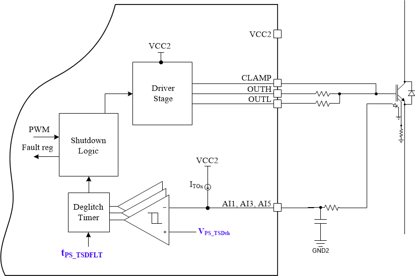
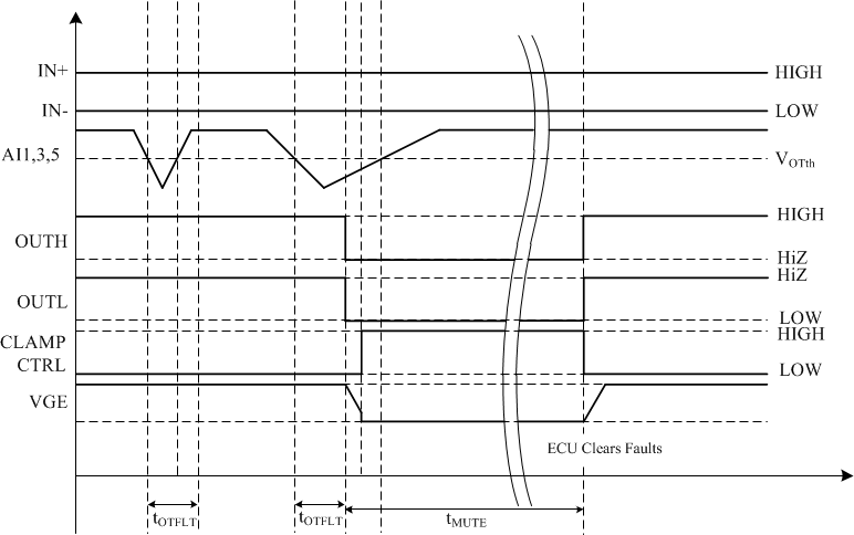
The device designates three AI* inputs (AI1, AI3, AI5) to support NTC diode sensing for up to three power transistors in parallel. The temperature protection is intended for power transistors with integrated temperature sensing diodes. The AI* input provides a zero-TC current that biases the integrated diode, and the voltage is monitored at the AI* input. The bias current is controlled using CFG3[ITO1_EN] (CFG3) as a master enable, and then using CFG3[AI_IZTC_SEL] (CFG3) to select which AI* output is to receive the bias current. Once the voltage at the AI* input falls below the threshold programmed using CFG6[TSD_PS] (CFG6), the fault is indicated in the STATUS3[PS_TSD_FAULT] (STATUS3), and if unmasked, nFLT1 is pulled low and the driver output goes to the state defined by CFG10[FS_STATE_PS_TSD] (CFG10). The turn-off of the driver output during an PS_TSD fault is selectable between normal, soft turn-off (STO), or two-level turnoff (2LTO) dictated by the CFG5[2LTOFF_STO_EN] bits. See the Section 7.3.5.9 and Section 7.3.5.8 for additional details on STO and 2LTO, respectively. Any PS_TSD fault must exist for the deglitch time programmed using the CFG4[PS_TSD_DEGLITCH] bits (CFG4) before the fault is registered. Enable/disable which AI* inputs are to be used for PS_TSD using the DOUTCFG[AI*PS_TSD_EN] bits (DOUTCFG). The temperature monitoring function is enabled for the selected AI* inputs using the CFG4[PS_PS_TEMP_EN] bit (CFG4). Please note that if AI5 is to be used for power switch temperature monitoring, the CFG8[AI_ASC_MUX] bit (CFG8) must be configured as an ADC input. The implementation diagram and timing schemes of PS_TSD are presented in Figure 7-20 and Figure 7-21 respectively.
 Figure 7-20 Block diagram of implementation of PS
temperature monitoring function.
 Figure 7-21 Timing scheme of implementation of
PS_TSD function.