SFFS094 April 2021 ISO6720 , ISO6720-Q1
4.1 8-D (narrow-body SOIC) and 8-DWV (wide-body SOIC) Package
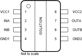
Figure 4-1 shows the ISO6720/ISO6720-Q1 and ISO6720F/ISO6720F-Q1 pin diagram for the 8-D and 8-DWV packages. For a detailed description of the device pins please refer to the Pin Configuration and Functions section in the ISO6720/ISO6720-Q1 data sheet.
 Figure 4-1 Pin Diagram (8-D and 8-DWV) Package
Table 4-2 Pin FMA for Device Pins Short-Circuited to
Ground
| Pin Name | Pin No. | Description of Potential Failure Effect(s) | Failure Effect Class |
|---|---|---|---|
| VCC1 | 1 | No power to the device on side-1. Observe that the absolute maximum ratings for all pins of the device are met; otherwise device damage may be plausible. | A |
| INA | 2 | Input signal shorted to ground, so output (OUTA) stuck to low. Communication from INA to OUTA corrupted. | B |
| INB | 3 | Input signal shorted to ground, so output (OUTB) stuck to low. Communication from INB to OUTB corrupted. | B |
| GND1 | 4 | Device continues to function as expected. Normal operation. | D |
| GND2 | 5 | Device continues to function as expected. Normal operation. | D |
| OUTB | 6 | OUTB stuck low. Data communication from INB to OUTB lost. Device damage possible if INB is driven high for extended period of time. | A |
| OUTA | 7 | OUTA stuck low. Data communication from INA to OUTA lost. Device damage possible if INA is driven high for extended period of time. | A |
| VCC2 | 8 | No power to the device on side-2. OUTA/OUTB pins state undetermined. | B |
Table 4-3 Pin FMA for Device Pins
Open-Circuited
| Pin Name | Pin No. | Description of Potential Failure Effect(s) | Failure Effect Class |
|---|---|---|---|
| VCC1 | 1 | Operation undetermined. Either device is unpowered and OUTA/OUTB=default logic state or through internal ESD diode on any IN pin, device can power up if any IN is driven to logic high. If IN pin has current sourcing capability to provide regular operating current of device, ESD diode conducts that current and device damage possible. | A |
| INA | 2 | No communication to INA channel possible. OUTA stuck to default state (High for ISO6720/ISO6720-Q1 and Low for ISO6720F/ISO6720F-Q1). | B |
| INB | 3 | No communication to INB channel possible. OUTB stuck to default state (High for ISO6720/ISO6720-Q1 and Low for ISO6720F/ISO6720F-Q1). | B |
| GND1 | 4 | Device unpowered on side1. OUTA/OUTB go to default state (High for ISO6720/ISO6720-Q1 and Low for ISO6720F/ISO6720F-Q1). | B |
| GND2 | 5 | Device unpowered on side-2. OUTA/OUTB state undetermined. | B |
| OUTB | 6 | State of OUTB undetermined. Data communication from INB to OUTB lost. | B |
| OUTA | 7 | State of OUTA undetermined. Data communication from INA to OUTA lost. | B |
| VCC2 | 8 | Device unpowered on side-2 and state of OUTA/OUTB undetermined. | B |
Table 4-4 Pin FMA for Device Pins Short-Circuited to
Adjacent Pin
| Pin Name | Pin No. | Shorted to | Description of Potential Failure Effect(s) | Failure Effect Class |
|---|---|---|---|---|
| VCC1 | 1 | INA | INA stuck high. External bit-stream for communication to INA pin corrupted. OUTA stuck high. | B |
| INA | 2 | INB | Communication corrupted for either INA or INB channel. | B |
| INB | 3 | GND1 | Input signal shorted to ground, so output (OUTB) stuck to low. Communication from INB to OUTB corrupted. | B |
| GND1 | 4 | INB | Already considered in above row. | B |
| GND2 | 5 | OUTB | OUTB pin stuck low. Communication corrupted. If IN pin is driven high for extended duration, OUTB pin stuck low creates a short between supply and ground with possible device damage. | A |
| OUTB | 6 | OUTA | Communication corrupted for either OUTA or OUTB channel. Device damage possible if INA and INB try to drive opposite logic state for extended duration creating a short between supply and ground on side-2. | A |
| OUTA | 7 | VCC2 | OUTA stuck high. Data communication from INA to OUTA lost. Device damage possible if INA is driven low for extended period of time. | A |
| VCC2 | 8 | OUTA | Already considered in above row. | A |
Table 4-5 Pin FMA for Device Pins Short-Circuited to
supply
| Pin Name | Pin No. | Description of Potential Failure Effect(s) | Failure Effect Class |
|---|---|---|---|
| VCC1 | 1 | No effect. Normal operation. | D |
| INA | 2 | INA pin stuck high. Communication corrupted. OUTA stuck high. | B |
| INB | 3 | INB pin stuck high. Communication corrupted. OUTB stuck high. | B |
| GND1 | 4 | Device side-1 unpowered. Observe that the absolute maximum ratings for INA/INB pins of the device are met, otherwise device damage may be plausible. | A |
| GND2 | 5 | Device side-2 unpowered. OUTA/OUTB state undetermined. | B |
| OUTB | 6 | OUTB stuck high. Communication disrupted. If INB is low for extended duration, OUTB being stuck high creates a short and can damage the device. | A |
| OUTA | 7 | OUTA stuck high. Communication disrupted. If INA is low for extended duration, OUTA being stuck high creates a short and can damage the device. | A |
| VCC2 | 8 | No effect. Normal operation. | D |