SLIB006A February 2011 – June 2021 TPS81256 , TPS82084 , TPS82085 , TPS82130 , TPS82140 , TPS82150 , TPS82670 , TPS82671 , TPS826711 , TPS826716 , TPS82672 , TPS826721 , TPS82673 , TPS82674 , TPS826745 , TPS82675 , TPS82676 , TPS826765 , TPS82677 , TPS8268090 , TPS8268105 , TPS8268120 , TPS8268150 , TPS8268180 , TPS82692 , TPS82693 , TPS82695 , TPS826951 , TPS82697 , TPS82698 , TPS82740A , TPS82740B , TPSM82810 , TPSM82813 , TPSM82816 , TPSM82821 , TPSM82821A , TPSM82822 , TPSM82822A , TPSM82823 , TPSM82823A
3.1 MicroSiP With BGA Pins
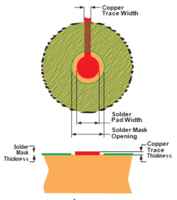
When designing the pads for MicroSiP devices with BGA pins, it is recommended that the layout use a non-solder mask defined (NSMD) pad. With this method, the solder mask opening is made larger than the desired land area, and the resulting copper size is defined solely by the size of the land pad of the device. Table 3-1 shows the appropriate pad design for MicroSiP™ devices with BGA pins. Specific recommendations are listed here and shown in Figure 3-1:
- Circuit traces from the NSMD PCB pads should be 75-µm to 100-µm wide in the exposed area inside the solder mask opening. Wider trace widths reduce device standoff, which worsens board level reliability (BLR).
- Best BLR results are achieved when the PCB laminate glass transition temperature is above the operating range of the application
- Recommended solder paste is Type 3 or Type 4
- For a PCB using a Ni/Au surface finish, the gold thickness should be less than 0.5 µm to avoid a reduction in thermal fatigue performance
- Solder mask thickness should be less than 20 µm on top of the copper circuit pattern, to increase device standoff and improve BLR
- Best solder stencil performance is achieved using laser cut stencils with electro-polishing. Use of chemically etched stencils gives inferior solder paste volume control.
| Land Pattern Dimensions | |||||
|---|---|---|---|---|---|
| Solder Pad Type | Land Pad Width | Solder Mask Opening | Copper Thickness | Stencil Opening | Stencil Thickness |
| Non-solder mask defined (NSMD) | 0.30 mm | 0.360 mm | 1 oz max (0.032 mm) | 0.34 mm diameter | 0.1 mm |

Figure 3-1 Recommended Pad Design for MicroSiP™ Devices With BGA Pins
See the device data sheet for specific recommendations.