ZHCSO42B December   2015  – July 2021 LM53625-Q1 , LM53635-Q1

PRODUCTION DATA  

  1. 特性
  2. 应用
  3. 说明
  4. Revision History
  5. Device Comparison
  6. Pin Configuration and Functions
  7. Specifications
    1. 7.1 Absolute Maximum Ratings
    2. 7.2 ESD Ratings
    3. 7.3 Recommended Operating Conditions
    4. 7.4 Thermal Information
    5. 7.5 Electrical Characteristics
    6. 7.6 System Characteristics
    7. 7.7 Timing Characteristics
    8. 7.8 Typical Characteristics
  8. Detailed Description
    1. 8.1 Overview
    2. 8.2 Functional Block Diagram
      1. 8.2.1 Control Scheme
    3. 8.3 Feature Description
      1. 8.3.1 RESET Flag Output
      2. 8.3.2 Enable and Start-Up
      3. 8.3.3 Soft-Start Function
      4. 8.3.4 Current Limit
      5. 8.3.5 Hiccup Mode
      6. 8.3.6 Synchronizing Input
      7. 8.3.7 Undervoltage Lockout (UVLO) and Thermal Shutdown (TSD)
      8. 8.3.8 Input Supply Current
    4. 8.4 Device Functional Modes
      1. 8.4.1 AUTO Mode
      2. 8.4.2 FPWM Mode
      3. 8.4.3 Dropout
      4. 8.4.4 Input Voltage Frequency Foldback
    5. 8.5 Spread-Spectrum Operation
  9. Application and Implementation
    1. 9.1 Application Information
    2. 9.2 Typical Applications
      1. 9.2.1 General Application
        1. 9.2.1.1 Design Requirements
        2. 9.2.1.2 Detailed Design Procedure
          1. 9.2.1.2.1 External Components Selection
            1. 9.2.1.2.1.1 Input Capacitors
              1. 9.2.1.2.1.1.1 Input Capacitor Selection
            2. 9.2.1.2.1.2 Output Inductors and Capacitors Selection
              1. 9.2.1.2.1.2.1 Inductor Selection
              2. 9.2.1.2.1.2.2 Output Capacitor Selection
          2. 9.2.1.2.2 Setting the Output Voltage
            1. 9.2.1.2.2.1 FB for Adjustable Versions
          3. 9.2.1.2.3 VCC
          4. 9.2.1.2.4 BIAS
          5. 9.2.1.2.5 CBOOT
          6. 9.2.1.2.6 Maximum Ambient Temperature
        3. 9.2.1.3 Application Curves
      2. 9.2.2 Fixed 5-V Output for USB-Type Applications
        1. 9.2.2.1 Design Requirements
        2. 9.2.2.2 Detailed Design Procedure
        3. 9.2.2.3 Application Curves
      3. 9.2.3 Fixed 3.3-V Output
        1. 9.2.3.1 Design Requirements
        2. 9.2.3.2 Detailed Design Procedure
        3. 9.2.3.3 Application Curves
      4. 9.2.4 Adjustable Output
        1. 9.2.4.1 Design Requirements
        2. 9.2.4.2 Detailed Design Procedure
        3. 9.2.4.3 Application Curves
    3. 9.3 What to Do and What Not to Do
  10. 10Power Supply Recommendations
  11. 11Layout
    1. 11.1 Layout Guidelines
    2. 11.2 Layout Example
  12. 12Device and Documentation Support
    1. 12.1 Device Support
      1. 12.1.1 第三方米6体育平台手机版_好二三四免责声明
    2. 12.2 Documentation Support
      1. 12.2.1 Related Documentation
    3. 12.3 接收文档更新通知
    4. 12.4 支持资源
    5. 12.5 Trademarks
    6. 12.6 Electrostatic Discharge Caution
    7. 12.7 术语表
  13. 13Mechanical, Packaging, and Orderable Information

Typical Characteristics

Unless otherwise specified the following conditions apply: VIN = 12 V, TA = 25°C. Specified temperatures are ambient.
GUID-1EB46B66-8BB3-40A1-85A9-2A1D50EA9D84-low.gif
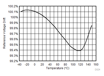
VIN = 12 V
Figure 7-1 Reference Voltage Drift
GUID-39F75759-A134-4255-9C8A-66CB5F9E89D0-low.gif
VIN = 12 V
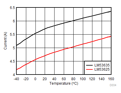
Figure 7-3 High Side/Peak Current Limit for LM53625/35-Q1
GUID-B5A3B357-5485-481F-897A-2A758D437BA0-low.gif
VIN = 12 V
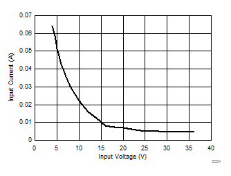
Figure 7-5 Short Circuit Average Input Current for LM53635-Q1
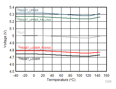
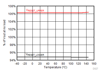
GUID-4D86450E-BE6D-42A9-AE3A-33804E4BB19F-low.gifFigure 7-7 RESET Threshold Fixed 5-V output
GUID-399BFBC3-06E3-4B71-99EB-72E733CC15EA-low.gif
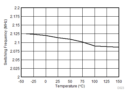
VIN = 12 V
Figure 7-2 Switching Frequency vs Temperature
GUID-B08A13B0-5717-4DC1-B015-A0D9DCCA5A6C-low.gif
VIN = 12V
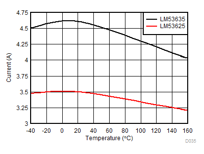
Figure 7-4 Low Side/Valley Current Limit for LM53625/35-Q1
GUID-59EFD78F-417D-4A86-AAE7-3B9C4E970652-low.gif
VIN = 12 V
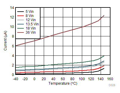
Figure 7-6 Shutdown Current
GUID-83053D91-BC7C-4B91-B28F-3A08A800CE47-low.gifFigure 7-8 RESET Threshold as Percentage of Output Voltage