ZHCSO42B December   2015  – July 2021 LM53625-Q1 , LM53635-Q1

PRODUCTION DATA  

  1. 特性
  2. 应用
  3. 说明
  4. Revision History
  5. Device Comparison
  6. Pin Configuration and Functions
  7. Specifications
    1. 7.1 Absolute Maximum Ratings
    2. 7.2 ESD Ratings
    3. 7.3 Recommended Operating Conditions
    4. 7.4 Thermal Information
    5. 7.5 Electrical Characteristics
    6. 7.6 System Characteristics
    7. 7.7 Timing Characteristics
    8. 7.8 Typical Characteristics
  8. Detailed Description
    1. 8.1 Overview
    2. 8.2 Functional Block Diagram
      1. 8.2.1 Control Scheme
    3. 8.3 Feature Description
      1. 8.3.1 RESET Flag Output
      2. 8.3.2 Enable and Start-Up
      3. 8.3.3 Soft-Start Function
      4. 8.3.4 Current Limit
      5. 8.3.5 Hiccup Mode
      6. 8.3.6 Synchronizing Input
      7. 8.3.7 Undervoltage Lockout (UVLO) and Thermal Shutdown (TSD)
      8. 8.3.8 Input Supply Current
    4. 8.4 Device Functional Modes
      1. 8.4.1 AUTO Mode
      2. 8.4.2 FPWM Mode
      3. 8.4.3 Dropout
      4. 8.4.4 Input Voltage Frequency Foldback
    5. 8.5 Spread-Spectrum Operation
  9. Application and Implementation
    1. 9.1 Application Information
    2. 9.2 Typical Applications
      1. 9.2.1 General Application
        1. 9.2.1.1 Design Requirements
        2. 9.2.1.2 Detailed Design Procedure
          1. 9.2.1.2.1 External Components Selection
            1. 9.2.1.2.1.1 Input Capacitors
              1. 9.2.1.2.1.1.1 Input Capacitor Selection
            2. 9.2.1.2.1.2 Output Inductors and Capacitors Selection
              1. 9.2.1.2.1.2.1 Inductor Selection
              2. 9.2.1.2.1.2.2 Output Capacitor Selection
          2. 9.2.1.2.2 Setting the Output Voltage
            1. 9.2.1.2.2.1 FB for Adjustable Versions
          3. 9.2.1.2.3 VCC
          4. 9.2.1.2.4 BIAS
          5. 9.2.1.2.5 CBOOT
          6. 9.2.1.2.6 Maximum Ambient Temperature
        3. 9.2.1.3 Application Curves
      2. 9.2.2 Fixed 5-V Output for USB-Type Applications
        1. 9.2.2.1 Design Requirements
        2. 9.2.2.2 Detailed Design Procedure
        3. 9.2.2.3 Application Curves
      3. 9.2.3 Fixed 3.3-V Output
        1. 9.2.3.1 Design Requirements
        2. 9.2.3.2 Detailed Design Procedure
        3. 9.2.3.3 Application Curves
      4. 9.2.4 Adjustable Output
        1. 9.2.4.1 Design Requirements
        2. 9.2.4.2 Detailed Design Procedure
        3. 9.2.4.3 Application Curves
    3. 9.3 What to Do and What Not to Do
  10. 10Power Supply Recommendations
  11. 11Layout
    1. 11.1 Layout Guidelines
    2. 11.2 Layout Example
  12. 12Device and Documentation Support
    1. 12.1 Device Support
      1. 12.1.1 第三方米6体育平台手机版_好二三四免责声明
    2. 12.2 Documentation Support
      1. 12.2.1 Related Documentation
    3. 12.3 接收文档更新通知
    4. 12.4 支持资源
    5. 12.5 Trademarks
    6. 12.6 Electrostatic Discharge Caution
    7. 12.7 术语表
  13. 13Mechanical, Packaging, and Orderable Information

Application Curves

The following characteristics apply only to the circuit of Figure 9-18. These parameters are not tested and represent typical performance only. Unless otherwise stated, the following conditions apply: VIN = 12 V, TA = 25°C. For the purpose of offering the more information to the designer, information for the application with FPWM pin high (FPWM mode) and FPWM pin low (AUTO mode) is included, although the schematic shows the application running specifically in AUTO mode. The mode is specified under each of the following graphs.
GUID-06A96154-D41B-4642-894A-A03658584366-low.gif
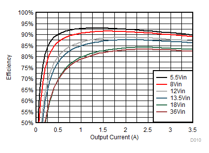
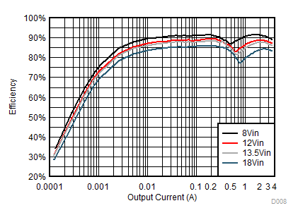
VOUT = 3.3 V AUTO
Figure 9-19 Efficiency
GUID-66371F8F-687A-4167-B7E8-07115D34B4FE-low.gif
VOUT = 3.3 V FPWM
Figure 9-21 Efficiency
GUID-FB8F799F-71DA-4060-A8A7-08C26934CC00-low.gif
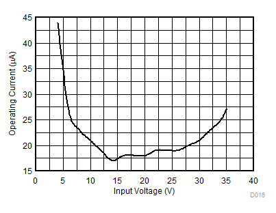
VOUT = 3.3 V AUTO IOUT = 0A
Figure 9-23 Input Supply Current (Includes Leakage Current of Capacitor)
GUID-39AF6B0F-C95B-4F7C-A772-E2F9B87BC87B-low.gif
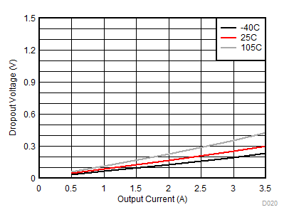
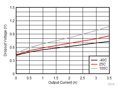
VOUT = 3.3 V
Figure 9-25 Dropout for –3% Regulation
GUID-9913062F-62BD-430C-9481-5A237556B157-low.gif
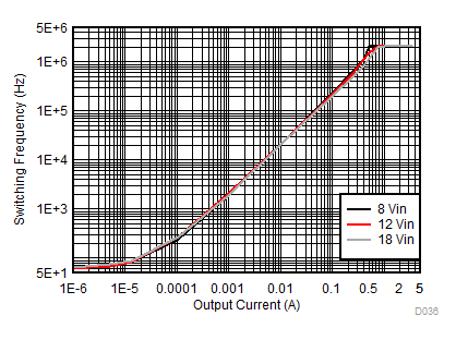
VOUT = 3.3 V AUTO
Figure 9-27 Switching Frequency vs Load Current
GUID-1E37DD1E-1743-4E7A-A613-9977176161E5-low.gif
VOUT = 3.3 V L=2.2 µH IOUT = 1 A
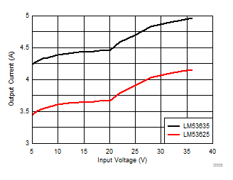
Figure 9-29 Output Current Level for Overcurrent Protection Trip
GUID-0AD1C86C-CBE1-4FA5-85A7-64D5D2B77478-low.png
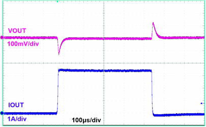
FPWM VOUT = 3.3 V L = 2.2 µH,
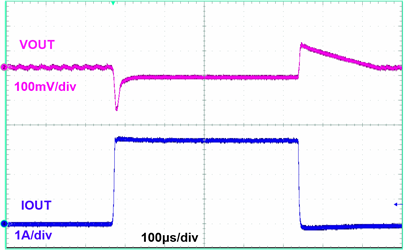
COUT = 3 × 22 µF IOUT = 0 A to 3.5 A TR = TF = 1 µs
Figure 9-31 Load Transient
GUID-5928F4E8-C152-4F66-96EF-7973D8263923-low.png
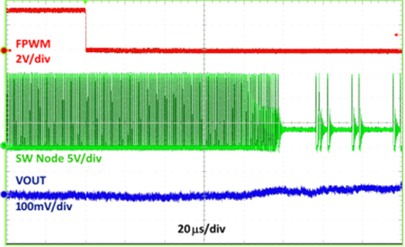
VOUT = 3.3 V IOUT = 10 mA
Figure 9-33 Mode Change Transient FPWM to AUTO Mode
GUID-C84A4F79-1E56-495E-970E-FA15010D71B9-low.gif
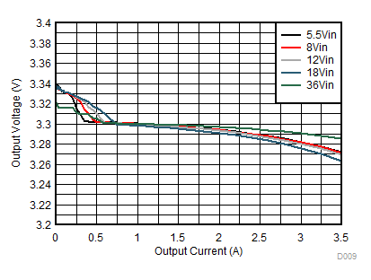
VOUT = 3.3 V AUTO
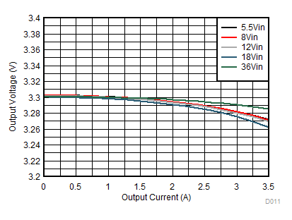
Figure 9-20 Load and Line Regulation
GUID-937D4A9A-917A-490D-8BCC-4DD63056D87D-low.gif
VOUT = 3.3 V FPWM
Figure 9-22 Load and Line Regulation
GUID-114359B5-C082-44B2-BBFF-248A9A99264F-low.gif
VOUT = 3.3 V
Figure 9-24 Load Current for PFM-to-PWM Transition
GUID-46510111-C3FF-42D4-86D4-CEB0BA029B25-low.gif
VOUT = 3.3 V
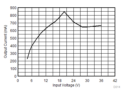
Figure 9-26 Dropout for ≥ 1.85 MHz
GUID-96E2B5D9-665B-450D-8B2C-74B5585659D5-low.gif
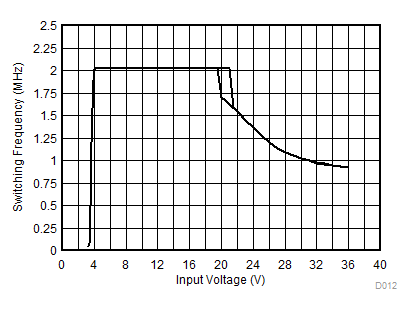
VOUT = 3.3 V FPWM IOUT = 1 A
Figure 9-28 Switching Frequency vs Input Voltage
GUID-2596A819-F5DE-43AC-9F21-9FD763E1C12C-low.png
AUTO VOUT = 3.3 V L = 2.2 µH,
COUT = 3 × 22 µF IOUT = 0 A to 3.5 A TR = TF = 1 µs
Figure 9-30 Load Transient
GUID-D2B9587B-66A3-4B3F-8CAA-033CDC536FB8-low.png
VOUT = 3.3 V IOUT = 10 mA
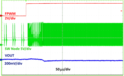
Figure 9-32 Mode Change Transient AUTO to FPWM mode