ZHCSO42B December 2015 – July 2021 LM53625-Q1 , LM53635-Q1
PRODUCTION DATA
- 1 特性
- 2 应用
- 3 说明
- 4 Revision History
- 5 Device Comparison
- 6 Pin Configuration and Functions
- 7 Specifications
- 8 Detailed Description
-
9 Application and Implementation
- 9.1 Application Information
- 9.2
Typical Applications
- 9.2.1 General Application
- 9.2.2 Fixed 5-V Output for USB-Type Applications
- 9.2.3 Fixed 3.3-V Output
- 9.2.4 Adjustable Output
- 9.3 What to Do and What Not to Do
- 10Power Supply Recommendations
- 11Layout
- 12Device and Documentation Support
- 13Mechanical, Packaging, and Orderable Information
封装选项
请参考 PDF 数据表获取器件具体的封装图。
机械数据 (封装 | 引脚)
- RNL|22
散热焊盘机械数据 (封装 | 引脚)
- RNL|22
订购信息
9.2.1 General Application
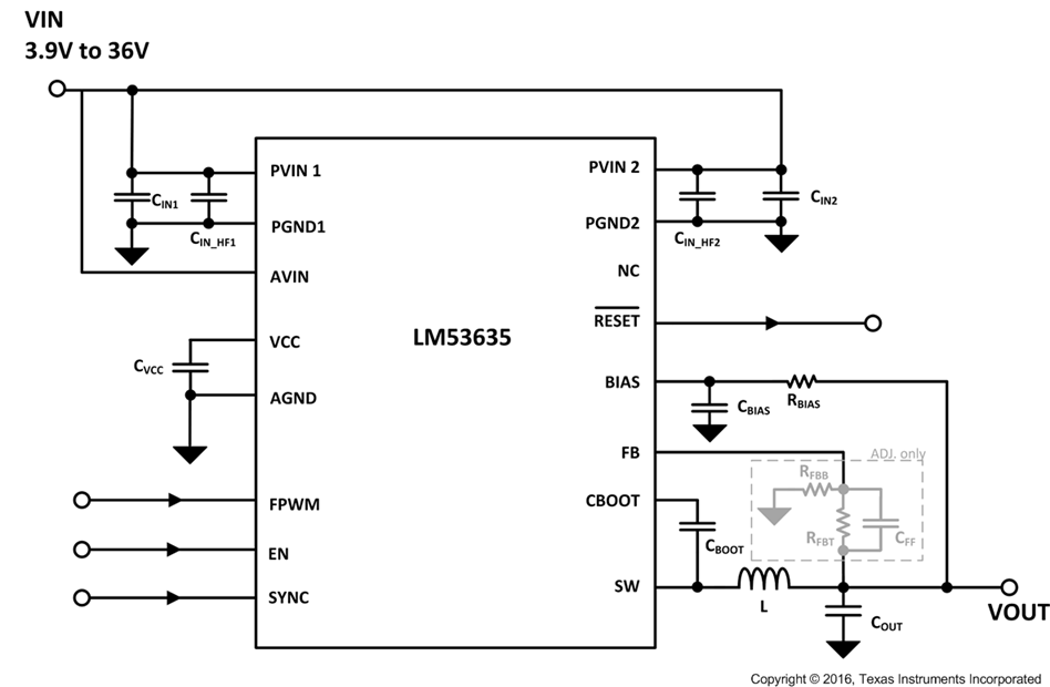
Figure 9-1 shows a general application schematic. FPWM, SYNC and EN are digital inputs. RESET is an open-drain output. FB connection is different for the fixed output options and the adjustable option.
- The FPWM pin can be connected to GND to enable light-load PFM operation. Select this option if current consumption at light load is critical. The pin can be connected to VCC or VIN for forced 2-MHz operation. Select this option if constant switching frequency is critical over the entire load range. The pin can also be driven by an external signal and can be toggled while the part is in operation (by an MCU for example.) Refer to the Section 7.5 and Section 8.4 for more details on the operation and signal requirements of the FPWM pin.
- The SYNC pin can be used to control the switching frequency and the phase of the converter. If the function is not needed, tie the SYNC pin to GND or 3 V.
- The RESET pin can be left floating if the function is not required. If the function is needed, the pin must be connected to a DC rail through a pullup resistor (100 kΩ is the typical recommended value). Check Section 7.5 and Section 8.3.1 for the details of the RESET-pin function.
- If the device is a fixed-output version (3.3 V or 5 V output option), connect the FB pin directly to the output. In the case of an adjustable-output part, connect the output to the FB pin through a voltage divider. See Section 9.2.1.2 for details on component selection.
- The BIAS pin can be connected directly to the output except in applications that can experience inductive shorts (such as cases with long leads on the output). In those cases, a 3 Ω or so is necessary between the output and the BIAS pin, and a small capacitor to GND is necessary close to the BIAS pin (CBIAS). Alternatively, a Schottky diode can be connected between the OUT and GND to limit the negative voltage that can arise on the output during inductive shorts. In addition, BIAS can also be connected to an external rail if necessary and if available. The typical current into the bias pin is 15 mA when the device is operating in PWM mode at 2.1 MHz.
- Power components must be chosen carefully for proper operation of the converter. Section 9.2.1.2 discusses the details of the process of choosing the input capacitors, output capacitors, and inductor for the application.
 Figure 9-1 General Application Circuit